

Determining how many MHz for RAM your enterprise infras […]
Determining how many MHz for RAM your enterprise infrastructure requires is often one of the most misunderstood decisions in server procurement. Hardware buyers regularly overspend on top-tier memory frequencies, only to face unexpected platform downclocking, thermal throttling, and budget waste in production. Balancing memory clock speed against architectural constraints solves this costly mismatch before hardware hits your data center racks.
For enterprise servers, the ideal RAM frequency is the highest native JEDEC speed your CPU and memory channel topology support without forced downclocking. Modern DDR4 platforms typically stabilize between 2933 MHz and 3200 MHz, while modern DDR5 deployments operate between 4800 MHz and 5600 MHz.[^1] Higher rated modules downclock if platform topology or slot population exceeds electrical limits.
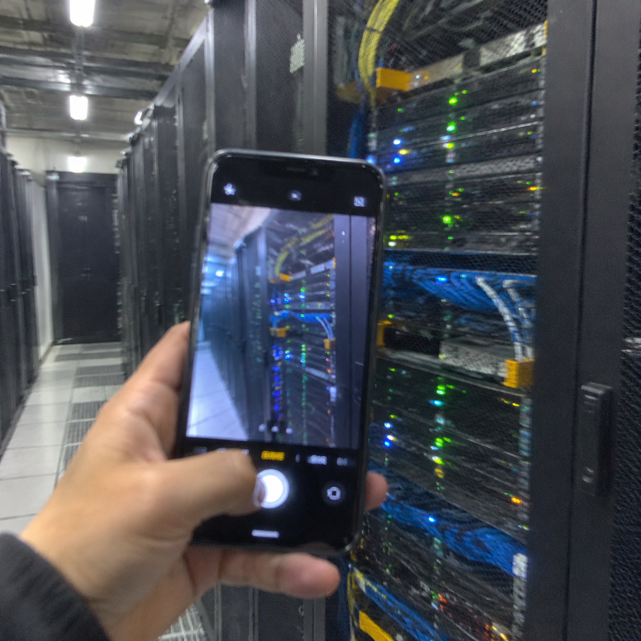
I frequently see systems deploy with expensive, high-frequency modules that quietly run underclocked from day one. To prevent this waste, you must examine how processors, motherboard slot densities, and real-world enterprise workloads govern practical memory performance.
Why Does CPU Platform Architecture Limit How Many MHz for RAM You Can Run?
Purchasing memory modules without cross-referencing integrated memory controller[^2] specs leads directly to silent system downgrades. Your procurement team buys premium silicon, yet your operating system reports lower operational frequencies across all nodes. Aligning your module selection with native CPU platform architecture prevents this frustrating loss of capital expenditure.
Your central processor's integrated memory controller dictates the absolute ceiling for RAM frequency based on JEDEC enterprise standards. Enterprise processors do not support consumer overclocking profiles. If you install 5600 MHz DIMMs on a processor certified only up to 4800 MHz, the system automatically runs the memory at 4800 MHz.
Integrated Memory Controller Constraints
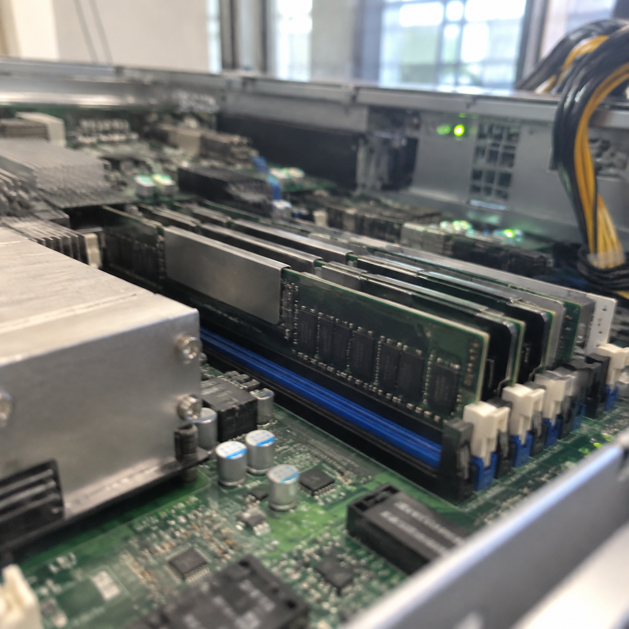
The processor architecture contains the integrated memory controller (IMC). The IMC manages data flow between CPU cores and system memory. In enterprise compute platforms like Intel Xeon and AMD EPYC, the IMC enforces strict voltage, timing, and frequency guardrails.
Consumer systems use extreme memory profiles like XMP or EXPO to bypass standard speeds. Enterprise platforms deliberately avoid these unstable overclocks. They run strictly on standard JEDEC profiles to ensure continuous uptime and absolute data integrity.
I regularly remind clients that server motherboards default to the lowest common denominator between the processor, the motherboard BIOS, and the memory module.
| CPU Generation | Memory Type | Maximum Native JEDEC Frequency | Typical Base Frequency |
|---|---|---|---|
| 2nd Gen Intel Xeon Scalable (Cascade Lake)[^3] | DDR4 RDIMM/LRDIMM | Up to 2933 MHz | 2400 / 2666 MHz |
| 3rd Gen Intel Xeon Scalable (Ice Lake) | DDR4 RDIMM/LRDIMM | Up to 3200 MHz | 2933 MHz |
| 4th Gen Intel Xeon Scalable (Sapphire Rapids)[^4] | DDR5 RDIMM | Up to 4800 MHz | 4400 MHz |
| 5th Gen Intel Xeon Scalable (Emerald Rapids) | DDR5 RDIMM | Up to 5600 MHz | 4800 / 5200 MHz |
| AMD EPYC 7003 Series (Milan) | DDR4 RDIMM | Up to 3200 MHz | 2666 / 3200 MHz |
| AMD EPYC 9004 Series (Genoa/Bergamo)[^5] | DDR5 RDIMM | Up to 4800 / 5200 MHz | 4800 MHz |
Motherboard Trace Routing and BIOS Validation
Motherboard physical construction also limits memory frequency. High-speed signal traces carry electrical pulses between the CPU socket and DIMM slots. As clock frequencies rise, electrical attenuation and crosstalk increase rapidly[^6].
High-layer server motherboards use premium PCB materials to preserve signal clarity. However, if the motherboard layout cannot maintain signal integrity at higher frequencies, the system BIOS forces lower operational speeds.
During our build validations at the OEM level, we routinely test motherboard Qualified Vendor Lists (QVL). We reject modules that cause signal degradation during multi-day stress runs, even when those modules run within nominal manufacturer specs.
How Does Memory Channel Topology Impact How Many MHz for RAM Are Delivered?
Designing high-capacity servers often demands populating every available memory slot across multi-channel motherboards. However, filling these slots adds significant capacitance to the memory bus, creating severe signal degradation. Understanding your memory channel topology prevents surprising drops in memory bus speed after deployment.
Memory channel topology directly determines operational frequency through slot density. When you run one DIMM per channel (1DPC), the platform runs at full rated JEDEC frequency. When you populate two DIMMs per channel (2DPC), the platform often downclocks the memory frequency to maintain signal stability.[^7]
The 1DPC vs. 2DPC Penalty
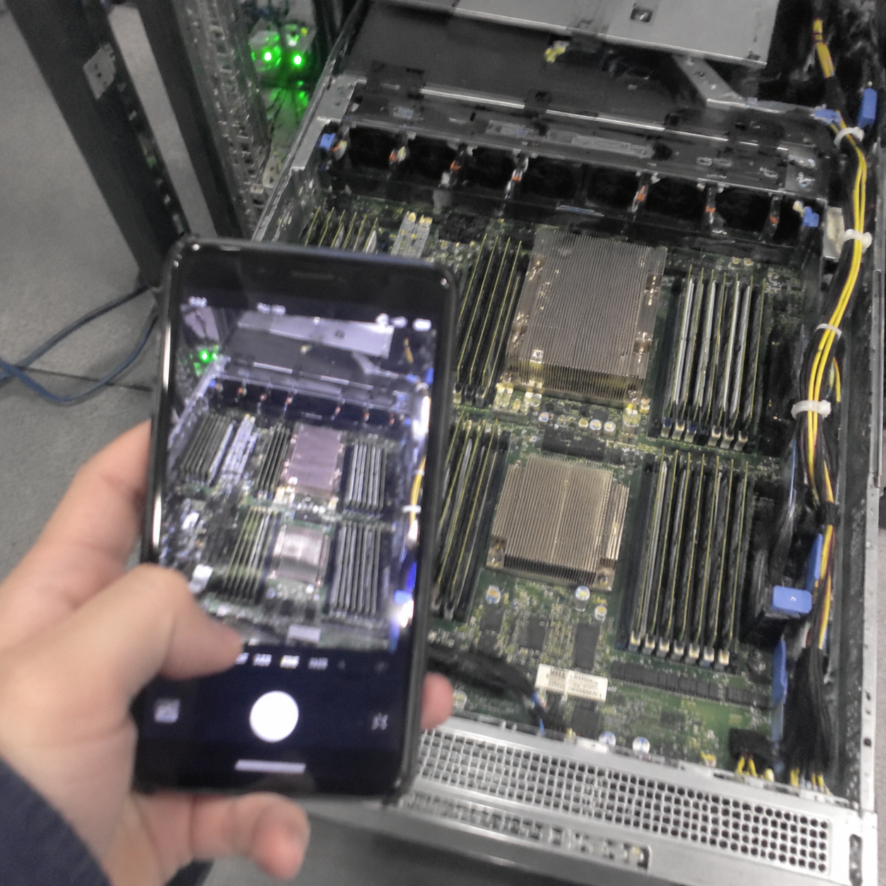
Modern server processors feature multi-channel memory architectures with 8 or 12 memory channels per socket. Motherboard designers can route either one DIMM slot per channel (1DPC) or two DIMM slots per channel (2DPC).
A 1DPC configuration maintains clean electrical traces and sharp signal edges. This setup allows the system to achieve its maximum certified frequency.
When you insert a second module on the same channel in a 2DPC configuration, you increase trace capacitance. The memory controller must work harder to drive electrical signals across multiple physical modules. To preserve enterprise-grade stability, the platform firmware automatically drops the operational frequency.
- 1DPC DDR5 configuration: Operates up to 4800 MT/s or 5600 MT/s cleanly across all active channels.
- 2DPC DDR5 configuration: Often downclocks automatically to 4400 MT/s or 4000 MT/s, depending on CPU stepping and rank count.
- Rank mixing impact: Mixing single-rank, dual-rank, or quad-rank DIMMs on a shared channel increases the electrical load further, triggering deeper frequency rollbacks.[^8]
Real-World Downclocking Case Study
I worked with a regional cloud service provider who ordered 200 compute nodes. The procurement team purchased 5600 MHz DDR5 modules to maximize throughput. They populated every slot in a 2DPC layout to reach 1.5 TB of RAM per node.
Once deployed, the systems automatically settled at 4400 MHz. The customer assumed the memory modules were defective.
In reality, the hardware operated exactly as intended by the CPU architectural guidelines. The customer had paid a 25% premium for 5600 MHz silicon that could never run past 4400 MHz in their chosen density configuration. Selecting 4800 MHz modules from the start would have saved tens of thousands of dollars without costing a single cycle of real-world performance.
Does Workload Performance Justify Paying for Higher MHz for RAM?
Procurement teams frequently assume that higher memory frequencies create linear gains in application throughput. This assumption leads to inflated bills of materials that strain capital budgets without improving service delivery. Evaluating the true relationship between memory bandwidth, latency, and real workload demands prevents wasteful hardware over-provisioning.
Typical enterprise workloads like virtualization, web hosting, and relational databases show minimal performance gains from marginal memory frequency increases. Raw bandwidth expands with higher MHz, but latency can increase simultaneously. Most business applications benefit far more from larger total capacity and balanced multi-channel configurations than from peak clock speeds.
Bandwidth vs. Latency Realities
Memory performance depends on two metrics: bandwidth and true latency. Frequency (measured in MHz or mega-transfers per second) dictates theoretical peak bandwidth. It indicates how much data can move across the bus in a second.
True operational latency represents the time required to locate and retrieve a specific piece of data. Latency is calculated using frequency alongside Column Address Strobe (CAS) latency:
$$text{True Latency (ns)} = frac{text{CAS Latency} times 2000}{text{Data Rate (MT/s)}}$[^9]$
As memory frequencies increase across JEDEC generations, CAS latency numbers rise as well. As a result, the true access latency in nanoseconds has remained relatively flat from late-generation DDR4 to mainstream DDR5.
[DDR4-3200 CL22: True Latency ≈ 13.75 ns](https://linustechtips.com/topic/1273074-does-cas-latency-matter-in-memory-sticks-is-cl22-too-much/)[^10]
DDR5-4800 CL40: True Latency ≈ 16.67 ns
DDR5-5600 CL46: True Latency ≈ 16.43 ns
Workload Sensitivity Profiles
Different enterprise workloads respond differently to changes in memory frequency:
- Virtualization clusters (VMware ESXi, Proxmox, KVM): These environments are heavily capacity-bound. A hypervisor benefits significantly from having enough gigabytes to avoid disk paging. It gains almost nothing from moving from 4800 MHz to 5600 MHz.
- Relational databases (SQL Server, PostgreSQL): Database engines rely heavily on random lookups. They depend on fast storage caches and low memory access latency. Marginal frequency bumps yield negligible query response gains.
- High-Performance Computing (HPC) and AI training: Computational fluid dynamics, linear algebra solvers, and large language model training push memory channels to maximum throughput. These specific workloads actively benefit from higher MHz because they saturate memory pipelines with continuous, parallel data streams.
Thermal and Power Penalties
Higher memory frequencies demand higher power and create more heat. A server chassis containing 32 DDR5 DIMMs generates substantial thermal load.
Operating memory at elevated frequencies raises module temperatures. Cooling those modules requires higher fan RPMs, which raises constant parasitic energy use. For large-scale data center operators, the added operational expense of cooling high-speed DIMMs can outweigh minor throughput benefits.
How Do Procurement Teams Calculate How Many MHz for RAM to Specify?
Sourcing memory without a systematic validation process introduces severe delivery delays, compatibility failures, and RMA disputes. Enterprise buyers must navigate conflicting specs between component vendors and assembly partners. Following an established hardware dependency chain ensures you specify the exact right speed every time.
Calculate your required memory frequency by mapping your hardware dependency chain from the top down. Start with your application's bandwidth sensitivity, verify the CPU's native memory frequency limits, review the motherboard's Qualified Vendor List, and calculate the density derating for your target slot population.
The 4-Step Hardware Dependency Chain
To ensure predictable hardware delivery, follow this rigorous evaluation sequence before signing purchase orders:
Step 1: Workload Needs Assessment
Categorize your software stack. If your applications are capacity-driven (such as microservices or standard virtualization), target mainstream, high-volume JEDEC frequencies. If your application is genuinely bandwidth-bound (such as HPC scientific modeling), identify whether the performance gain justifies premium modules.
Step 2: CPU Platform Verification
Consult the official processor technical documentation. Identify the maximum native frequency supported by the processor's IMC. Never purchase memory rated above this baseline unless you have confirmed a specific platform feature that utilizes it.
Step 3: Slot Population Analysis
Map your desired memory capacity against available motherboard slots:
- If you achieve your target capacity using one DIMM per channel (1DPC), you can safely source modules at the processor's maximum rated frequency.
- If your capacity requirements require two DIMMs per channel (2DPC), check the platform's downclocking table. Specify modules that match the lower downclocked frequency to reduce BOM costs.
Step 4: QVL and Vendor Cross-Checking
Check the motherboard vendor's Qualified Vendor List (QVL) for verified part numbers. The QVL proves that a module completed physical electrical testing on that specific board design.
In our ODM manufacturing facility, we verify that the module's programmable SPD (Serial Presence Detect) chip[^11] matches the platform BIOS firmware. This check prevents POST initialization boot loops in production.
Evaluating Supplier Competence
When selecting an OEM/ODM manufacturing partner, evaluate how they handle memory specifications. A commodity vendor will simply sell you the most expensive module you ask for. A reliable engineering partner will review your topology and question an over-specified frequency.
Request full platform validation reports from your supplier. Ensure your supplier tests memory under full thermal loads inside your target chassis design. Verifying module performance in real rack conditions is the ultimate test of system stability.
Frequently Asked Questions
What happens if I install RAM with higher MHz than my server CPU supports?
Your server will boot and operate normally in most cases, but the memory controller will downclock the modules to match the CPU's native ceiling. You will pay for high-frequency capability without receiving any functional performance benefits.
Is DDR5 RAM always faster than DDR4 RAM in enterprise environments?
DDR5 provides significantly higher raw bandwidth than DDR4 by utilizing higher frequencies and dual sub-channels per DIMM[^12]. However, its initial access latency is comparable to DDR4. Workloads that depend on raw data throughput benefit noticeably, while latency-bound workloads show smaller improvements.
Can I mix different RAM frequencies within the same server motherboard?
You can mix frequencies physically, but it is not recommended for enterprise servers. The motherboard BIOS will automatically downclock all installed modules to the frequency of the slowest DIMM. Mixing speeds can also cause timing mismatches and system instability.
Why does memory speed drop when I fill all server DIMM slots?
Filling all slots puts two DIMMs on a single channel (2DPC). This increases the electrical capacitance on the trace lines. The processor downclocks the memory frequency to preserve clean signal integrity and prevent data corruption.
Conclusion
Choosing the right memory speed is an architectural balancing act rather than an exercise in chasing peak numbers. The correct answer to how many MHz for RAM your infrastructure needs depends entirely on your processor limits, channel topology, and target workloads. Prioritizing system stability and platform validation ensures reliable data center deployments.
At our enterprise manufacturing facilities, we guide global integrators and data center operators through complete system-level validation. We align processor capabilities, custom board traces, and certified memory modules to match your exact budget and performance requirements. Contact our engineering team today to review your hardware specifications and optimize your server deployment pipeline.
[^1]: "DDR5 SDRAM", https://en.wikipedia.org/wiki/DDR5_SDRAM. JEDEC standard publications JESD79-4 and JESD79-5 define the operational data rates for DDR4 up to 3200 MT/s and DDR5 starting at 4800 MT/s through mainstream ratings including 5600 MT/s. Evidence role: expert_consensus; source type: institution. Supports: Standard JEDEC speed definitions and baseline frequency ranges for DDR4 and DDR5 memory modules.. Scope note: JEDEC standards define theoretical timing and electrical profiles; actual server operational speed depends on the installed processor's memory controller support. [^2]: "JEDEC STANDARD", https://ptacts.uspto.gov/ptacts/public-informations/petitions/1558373/download-documents?artifactId=aNsaJtdk3pmW9ioNxVDBBIVNxw6-SCJpH10rjfEtG5NFu9EVHsN3eZ0. Technical architecture references explain how integrated memory controllers enforce signal integrity and JEDEC timings across multi-channel interfaces to prevent data corruption. Evidence role: mechanism; source type: research. Supports: The role and architectural function of the integrated memory controller in regulating memory frequency, timings, and voltage to JEDEC standards.. Scope note: Hardware controller implementations vary between microarchitectural designs and processor vendor generations. [^3]: "Cascade Lake", https://en.wikipedia.org/wiki/Cascade_Lake. Technical documentation for 2nd Gen Intel Xeon Scalable processors confirms native memory subsystem support up to DDR4-2933 across six memory channels per socket. Evidence role: statistic; source type: research. Supports: The maximum rated native DDR4 memory operating frequency supported by 2nd Generation Intel Xeon Scalable processors.. Scope note: Attaining 2933 MT/s on Cascade Lake requires compatible platinum/gold tier SKUs and 1DPC or specific RDIMM topologies. [^4]: "Sapphire Rapids", https://en.wikipedia.org/wiki/Sapphire_Rapids. Platform documentation for 4th Gen Intel Xeon Scalable processors confirms official memory support for up to DDR5-4800 in single-DIMM-per-channel configurations across eight channels. Evidence role: statistic; source type: research. Supports: The native DDR5 memory speed limits established for 4th Generation Intel Xeon Scalable systems.. Scope note: Subsequent firmware revisions and specific processor stepping levels dictate exact multi-channel downclock thresholds under 2DPC. [^5]: "DDR5 SDRAM", https://en.wikipedia.org/wiki/DDR5_SDRAM. AMD EPYC 9004 Series processor documentation specifies 12 memory channels natively accommodating DDR5 RDIMMs up to 4800 MT/s, with select models certified up to 5200 MT/s. Evidence role: statistic; source type: research. Supports: The supported native memory frequencies across the 12-channel memory controller of AMD EPYC 9004 series processors.. Scope note: The higher 5200 MT/s speed is restricted to specific EPYC SKUs and strict 1DPC motherboard routing requirements. [^6]: "High-Speed PCB Design Guide", https://s3vi.ndc.nasa.gov/ssri-kb/static/resources/High-Speed%20PCB%20Design%20Guide.pdf. Studies in high-speed digital transmission demonstrate that increased clock frequencies amplify dielectric losses and trace coupling, necessitating tighter signal integrity budgets. Evidence role: mechanism; source type: paper. Supports: The electrical phenomena of dielectric loss, conductor skin effect, and capacitive crosstalk worsening with increased memory bus clock frequencies.. Scope note: The degree of signal degradation is dependent upon PCB trace geometry, dielectric constant, and board layering rather than frequency alone. [^7]: "Multi-channel memory architecture", https://en.wikipedia.org/wiki/Multi-channel_memory_architecture. Electrical engineering design guides detail how secondary DIMM loads introduce stub reflections and parasitic capacitance, compelling memory controllers to step down clock rates to preserve eye margins. Evidence role: mechanism; source type: education. Supports: The mechanism whereby electrical loading in multi-drop bus topologies degrades eye height and forces frequency reductions.. Scope note: Modern systems utilizing point-to-point topologies or advanced multiplexing buffers may exhibit different derating curves. [^8]: "derating for eee-inst-002", https://snebulos.mit.edu/projects/crater/docs/engineering/EEE-parts-derating.pdf. Server system integration manuals establish strict rank-mixing population rules, noting that multi-rank configurations introduce additional chip select loads that require lower operating frequencies. Evidence role: mechanism; source type: research. Supports: How the accumulation of physical ranks on a single channel increases electrical loading on the command/address bus and requires frequency step-downs.. Scope note: Specific downclock thresholds depend on whether registered (RDIMM) or load-reduced (LRDIMM) modules are used, as buffer architectures alter the effective bus loading. [^9]: "CAS latency", https://en.wikipedia.org/wiki/CAS_latency. Computer systems engineering references define absolute read latency as the product of CAS latency and clock period, expressed algebraically as (CL × 2000) / Data Rate (MT/s). Evidence role: definition; source type: education. Supports: The standard formula converting synchronous clock cycles of CAS latency into absolute time measured in nanoseconds.. Scope note: This formula isolates the initial Column Address Strobe delay and excludes memory controller queuing delays, command overhead, and round-trip transport times. [^10]: "does cas latency matter in memory sticks? (is CL22 too much?)", https://linustechtips.com/topic/1273074-does-cas-latency-matter-in-memory-sticks-is-cl22-too-much/. JEDEC standard JESD79-4 specifications for DDR4-3200 speed bins define standard CL22 timing, which equates to an effective column access duration of approximately 13.75 nanoseconds. Evidence role: statistic; source type: institution. Supports: The baseline first-word timing calculation for standard JEDEC DDR4-3200 speed bins operating at CAS Latency 22.. Scope note: The metric represents theoretical first-word access time under open-page hit conditions and does not reflect average memory subsystem latency during page misses. [^11]: "Serial presence detect", https://en.wikipedia.org/wiki/Serial_presence_detect. JEDEC standard JESD21-C specifies the Serial Presence Detect (SPD) data structure, detailing how platform BIOS queries the SPD EEPROM to initialize memory clock rates and timings at boot. Evidence role: definition; source type: institution. Supports: The role and standardized function of the Serial Presence Detect (SPD) non-volatile memory device in communicating module timing parameters during platform initialization.. Scope note: Platform BIOS implementations can override SPD profile data depending on custom board policies and manual firmware configurations. [^12]: "DDR5 SDRAM", https://en.wikipedia.org/wiki/DDR5_SDRAM. JEDEC standard JESD79-5 details the architectural shift in DDR5 to two independent 32-bit (plus 8-bit ECC) sub-channels per DIMM, enhancing memory bus concurrency and channel efficiency. Evidence role: mechanism; source type: institution. Supports: The architectural transition in DDR5 from a single 64-bit data channel to two independent 32-bit sub-channels per DIMM.. Scope note: While dual sub-channels enhance parallel transactional efficiency, overall throughput remains bound by integrated memory controller scheduler utilization.
发表回复