

Enterprise server deployments often suffer unexpected l […]
Enterprise server deployments often suffer unexpected latency spikes and application bottlenecks when system memory is poorly configured. IT infrastructure teams frequently blame processor limits when the hidden culprit is an improperly configured memory subsystem. Understanding the actual bandwidth of RAM reveals the true hardware ceiling, ensuring your enterprise infrastructure delivers predictable, non-blocking performance across demanding multi-tenant compute environments.
The bandwidth of RAM represents the maximum theoretical rate at which data transfers between the processor and system memory, calculated as Transfer Rate (MT/s) multiplied by Bus Width (8 bytes per channel) multiplied by Active Channels. In enterprise servers, multi-channel architectures scale this rate from roughly 25.6 GB/s per DIMM up to over 300–460 GB/s[^1].
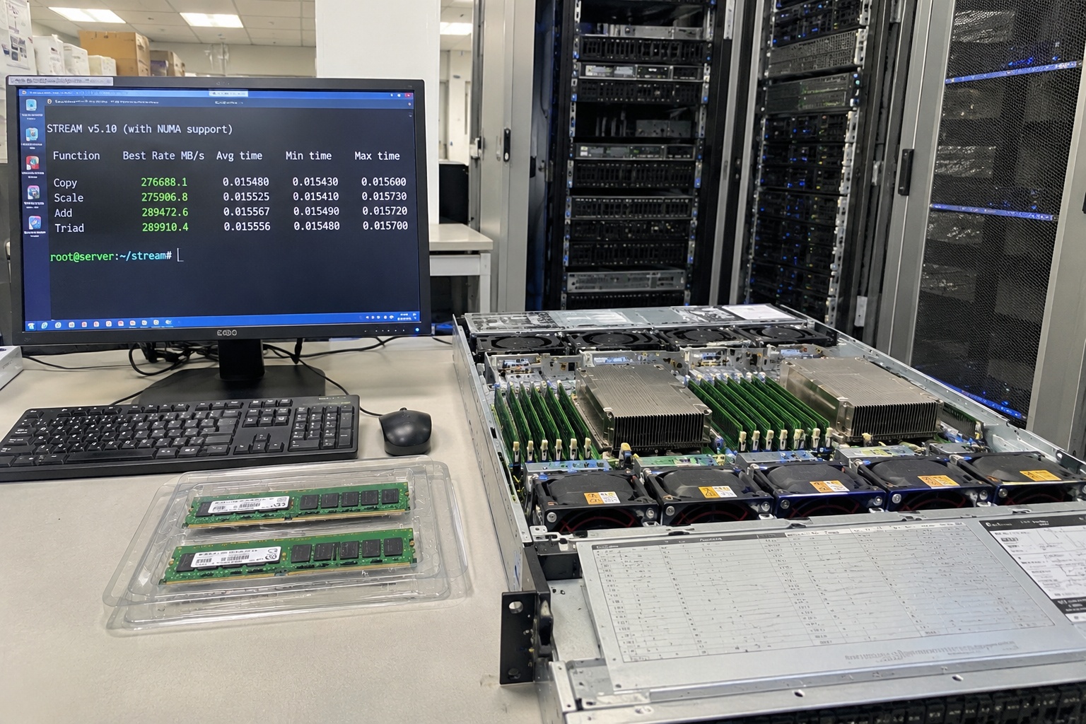
Evaluating component data sheets is only the starting point for infrastructure procurement leads and system integrators. To prevent expensive overprovisioning and avoid architectural choke points across your server deployments, we must examine how physical channels, architectural latencies, and bus topologies dictate real-world memory performance.
How do you calculate the theoretical bandwidth of RAM?
Component spec sheets often overwhelm hardware procurement teams with disconnected metrics like megahertz, megatransfers, and CAS latencies. Without a standardized formula, you risk misjudging whether a memory subsystem can satisfy multi-core processor demands. Calculating the theoretical bandwidth of RAM establishes an objective performance baseline during the technical evaluation of server components.
To calculate the theoretical bandwidth of RAM, multiply the data transfer rate in megatransfers per second (MT/s) by the bus width (8 bytes for a standard 64-bit channel), then multiply by the total active memory channels. For instance, a single DDR4-3200 channel delivers a theoretical peak of 25.6 GB/s ($3200 times 8 times 1$).
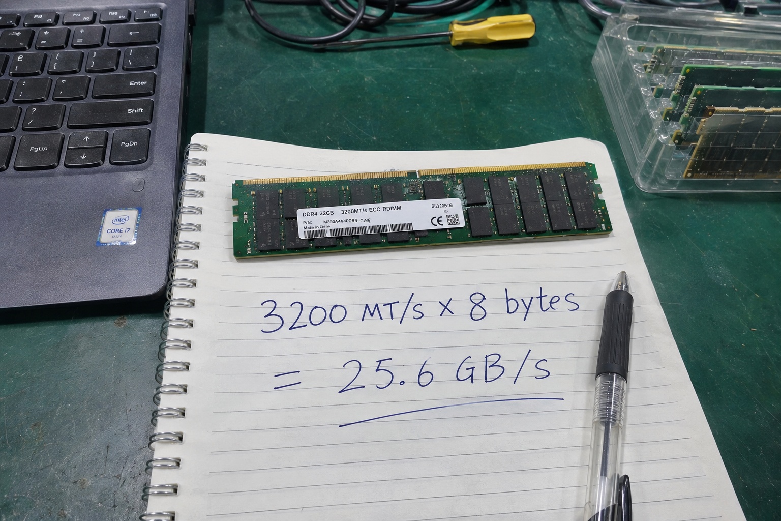
The Mathematical Formula
When sizing platforms for enterprise clients, I always guide engineers back to the fundamental physical equation governing memory bus architectures:
$$text{Theoretical Peak Bandwidth (MB/s)} = text{Data Transfer Rate (MT/s)} times left(frac{text{Bus Width in Bits}}{8}right) times text{Memory Channels}$$
To express this value in gigabytes per second (GB/s), divide the product by 1,000 (decimal standard) or 1,024 (binary standard). Most component manufacturers and silicon vendors publish specifications using the decimal standard ($1 text{ GB/s} = 1,000 text{ MB/s}$).
Demystifying MT/s vs. MHz
A common procurement pitfall is confusing clock frequency (MHz) with data rate (MT/s). Modern system memory operates on Double Data Rate (DDR) architecture, which transfers data on both the rising and falling edges of the clock cycle[^2].
- A DDR4 memory module running at an actual I/O clock frequency of 1600 MHz executes transfers at 3200 MT/s.
- A standard single memory channel operates across a 64-bit wide data bus (excluding parity/ECC lines).
- Since 64 bits equal 8 bytes, every clock cycle transfers 8 bytes of data per channel.
| Generation & Speed Grade | I/O Clock Frequency | Data Transfer Rate | Single-Channel Peak Bandwidth | Dual-Channel Peak Bandwidth |
|---|---|---|---|---|
| DDR4-2400 | 1200 MHz | 2400 MT/s | 19.2 GB/s | 38.4 GB/s |
| DDR4-2933 | 1466.5 MHz | 2933 MT/s | 23.46 GB/s | 46.93 GB/s |
| DDR4-3200 | 1600 MHz | 3200 MT/s | 25.6 GB/s | 51.2 GB/s |
| DDR5-4800 | 2400 MHz | 4800 MT/s | 38.4 GB/s | 76.8 GB/s |
| DDR5-5600 | 2800 MHz | 5600 MT/s | 44.8 GB/s | 89.6 GB/s |
| DDR5-6400 | 3200 MHz | 6400 MT/s | 51.2 GB/s | 102.4 GB/s |
During our hardware spec reviews, I frequently encounter client inquiries equating the transfer rate directly to system execution speed. In reality, a single high-speed module can easily choke a modern 32-core or 64-core enterprise processor if the channel configuration fails to feed all processing threads simultaneously.
Why does real-world throughput fall below the bandwidth of RAM?
Sizing production server nodes based strictly on theoretical peak ratings inevitably leads to degraded application response times. When enterprise databases or hypervisors hit memory bottlenecks under load, operations stall unexpectedly. Understanding why usable throughput falls below the theoretical bandwidth of RAM protects engineering teams from underprovisioning critical computing resources.
Real-world throughput falls below the theoretical bandwidth of RAM because protocol overhead, command bus contention, memory refresh cycles, and Non-Uniform Memory Access (NUMA) traversal consume link resources. As a result, enterprise server workloads typically achieve between 70% and 85% of theoretical peak bandwidth[^3] under sustained operational conditions.
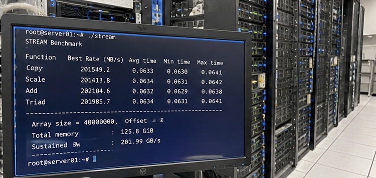
Protocol Overhead and Command Latency
Memory cells cannot transmit data continuously. Dynamic Random-Access Memory (DRAM) requires constant management commands that interrupt continuous data bursts:
- Row Access and Precharge Delays: Data inside DRAM chips is arranged in rows and columns. Opening a row requires precharging and activation phases (governed by timings like $t{RCD}$ and $t{RP}$). Switching between different rows introduces idle cycles on the data bus.
- Read/Write Turnaround Delays: The physical memory bus cannot execute read and write operations at the same exact microsecond. Reversing the signal direction requires bus turnaround penalties ($t_{WTR}$), reducing overall channel efficiency during mixed-operation workloads.
- Periodic Refresh Cycles ($t_{RFC}$): DRAM capacitors leak electrical charge. The memory controller must periodically halt standard operations to recharge internal cells across every bank, shaving off 3% to 5% of theoretical availability[^4].
NUMA Topology and Inter-Socket Penalties
Modern multi-socket server platforms distribute physical memory channels across discrete processor sockets in a Non-Uniform Memory Access (NUMA) topology.
When a thread executing on CPU Socket 0 attempts to access memory directly wired to CPU Socket 1, the transaction must traverse an inter-socket coherency link (such as Intel UPI or AMD Infinity Fabric).
This cross-socket hop adds significant command latency (often 50–100 nanoseconds[^5]) and restricts usable throughput down to the maximum transmission speed of the inter-socket fabric. In poorly tuned virtualization clusters, high rates of remote NUMA node access can degrade effective memory bandwidth by 30% or more[^6] compared to local node access.
How do memory channels scale the total bandwidth of RAM?
Purchasing premium memory modules while neglecting channel topology is one of the most common configuration errors in enterprise hardware procurement. Deploying memory in an unbalanced configuration throttles multi-core CPUs, regardless of how fast individual DIMMs run. Proper channel population scales the total bandwidth of RAM across enterprise platforms to match multi-threaded compute demands.
Populating additional independent memory channels scales the aggregate bandwidth of RAM linearly. An eight-channel server platform running DDR4-3200 delivers an aggregate theoretical ceiling of 204.8 GB/s ($25.6 times 8$), compared to just 25.6 GB/s for a single channel, directly multiplying bus throughput without increasing operating clock frequencies.
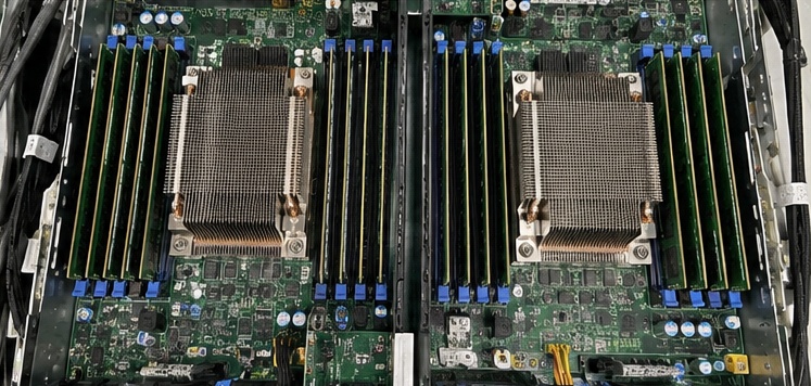
Linear Scaling Across Server Sockets
Desktop systems typically feature dual-channel controllers, but enterprise server platforms rely on quad-channel, 8-channel, or even 12-channel configurations per socket. Adding independent physical channels multiplies the data bus width by 64 bits per channel, providing dedicated, parallel data highways directly to the processor cache.
Single-Channel (64-bit bus)  --> [ 8 Bytes ] = 25.6 GB/s @ DDR4-3200
Dual-Channel   (128-bit bus) --> [ 16 Bytes ] = 51.2 GB/s @ DDR4-3200
Quad-Channel   (256-bit bus) --> [ 32 Bytes ] = 102.4 GB/s @ DDR4-3200
Eight-Channel  (512-bit bus) --> [ 64 Bytes ] = 204.8 GB/s @ DDR4-3200
Twelve-Channel (768-bit bus) --> [ 96 Bytes ] = 307.2 GB/s @ DDR4-3200
In technical client evaluations, I routinely demonstrate that a fully balanced 8-channel DDR4-2933 system (achieving ~187.7 GB/s theoretical) easily outpaces an unbalanced, dual-channel DDR5-4800 deployment (~76.8 GB/s theoretical) in multi-threaded enterprise workloads. Raw transfer rate per module cannot compensate for missing memory channels.
DIMMs Per Channel (DPC) and Speed Derating
Scaling capacity introduces physical trade-offs. Server mainboards typically offer either 1 DIMM Per Channel (1 DPC) or 2 DIMMs Per Channel (2 DPC).
- Signal Degradation: Attaching two physical memory modules to the same electrical trace increases capacitive loading and introduces signal reflections.
- Automatic Downclocking: To maintain signal integrity and prevent bit errors, processor memory controllers frequently force modules to operate at lower transfer rates when both slots in a channel are populated. For example, a platform rated for DDR5-4800 at 1 DPC may downclock to DDR5-4000 or DDR5-3600 at 2 DPC[^7].
Procurement teams must balance the need for gross memory capacity against the potential loss of memory bus throughput when filling every available DIMM slot.
How does DDR4 compare to DDR5 in the usable bandwidth of RAM?
Evaluating platform transitions between hardware generations requires analyzing structural architecture rather than just headline transfer numbers. Upgrading enterprise server nodes to DDR5 represents a major capital expenditure for data centers. Examining architectural revisions helps buyers verify whether the usable bandwidth of RAM justifies the migration cost for specific enterprise workloads.
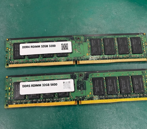
DDR5 substantially expands the usable bandwidth of RAM by splitting the traditional 64-bit data bus into two independent 32-bit subchannels per DIMM[^8], doubling the default burst length from 8 to 16[^9], and lifting base transfer rates to 4800–6400 MT/s, which dramatically reduces memory bus contention.
Architectural Subchannels and Concurrency
The fundamental structural difference between DDR4 and DDR5 lies in how data routes across the printed circuit board:
- DDR4 Architecture: Each standard DDR4 module features a single 64-bit wide data channel (plus an additional 8 bits for ECC, totaling 72 bits). A memory access cycle locks the entire 64-bit bus for that module.
- DDR5 Architecture: Each DDR5 module splits the bus into two independent 32-bit subchannels (plus 8 ECC bits each, totaling 40 bits per subchannel). Both subchannels operate independently, each featuring its own Command/Address (CA) pins.
This dual-subchannel architecture doubles memory access concurrency. While a single DDR5 module still transfers 64 data bits per cycle, it can execute two separate 32-byte read or write transactions simultaneously, perfectly matching modern CPU cache-line sizes (64 bytes) via doubled burst length (BL16).
Generational Architectural Comparison
| Architectural Feature | DDR4 Enterprise Standard | DDR5 Enterprise Standard | Operational Benefit |
|---|---|---|---|
| Bus Architecture per DIMM | $1 times 64text{-bit}$ channel | $2 times 32text{-bit}$ subchannels | Enables parallel transactions per module |
| Default Burst Length | BL8 (Burst Length 8) | BL16 (Burst Length 16) | Matches 64-byte processor cache lines cleanly |
| Bank Groups | 4 groups (16 banks total) | 8 groups (32 banks total) | Mitigates bank conflict latency |
| Power Management | Integrated on motherboard | Integrated on DIMM (PMIC)[^10] | Cleaner signal integrity at high MT/s |
| Base Transfer Rates | 2133 to 3200 MT/s | 4800 to 6400+ MT/s | Significant increase in raw bus speed |
| Error Checking Architecture | Sideband ECC across bus | On-Die ECC + Sideband ECC[^11] | Mitigates internal cell-level degradation |
In our engineering reviews of enterprise spec sheets, DDR5 modules consistently achieve higher operational bus utilization (often 80% to 90% in database workloads[^12]) compared to equivalent DDR4 modules, which often top out near 70% to 75% efficiency on identical access patterns.
Frequently Asked Questions
What is the difference between memory speed and memory bandwidth?
Memory speed refers to the frequency or transfer rate of the individual module (measured in MHz or MT/s), indicating how quickly data bits switch on the bus. Memory bandwidth represents the total volume of data moved per second across the entire system (measured in GB/s), which depends directly on bus width and active channel count.
Does adding more RAM increase the bandwidth of RAM?
Adding more RAM only increases the bandwidth of RAM if the additional modules populate previously empty memory channels. If your server platform has unpopulated memory channels, adding matching DIMMs increases total parallel data width. Adding modules to an already fully populated channel increases memory capacity, not bus bandwidth.
Why does high memory density sometimes lower memory operating speed?
High-density configurations often place multiple memory ranks and multiple DIMMs on the same physical channel. This configuration adds electrical load and capacitance to the trace lines. Server memory controllers automatically step down the transfer frequency to preserve signal integrity and avoid timing errors.
How does memory bandwidth impact virtualization and database workloads?
Virtualization hosts run numerous compute threads that execute unpredictable, concurrent read and write operations. High memory bandwidth ensures multiple virtual machines access the host memory bus simultaneously without forcing the CPU cores into wait states, directly lowering transaction latency and preventing virtual machine performance jitter.
Conclusion
Maximizing the usable bandwidth of RAM requires balancing component transfer speeds, memory channel population, NUMA topologies, and generational architectures. For enterprise infrastructure planners, prioritizing balanced multi-channel designs over isolated high-frequency modules ensures sustained compute throughput while mitigating thermal risks and operational stability concerns.
As an OEM/ODM hardware manufacturer specializing in server architecture, data center power systems, and edge compute platforms, we help systems integrators and enterprise operators design and manufacture fully validated, application-tailored server platforms. If you are planning an upcoming hardware deployment or require custom server manufacturing built around predictable memory throughput and scale, contact our engineering team to review your technical specifications.
[^1]: "DDR5 SDRAM", https://en.wikipedia.org/wiki/DDR5_SDRAM. Enterprise processor platform architectural briefs confirm that multi-channel memory subsystems (such as 8-channel and 12-channel configurations running DDR5-4800 to DDR5-6400) deliver theoretical aggregate throughput exceeding 300 to 460 GB/s. Evidence role: statistic; source type: institution. Supports: Multi-channel DDR5 server platforms scale aggregate peak bandwidth past 300–460 GB/s.. Scope note: Realized throughput depends on specific socket topology, channel population, and memory controller operational frequencies. [^2]: "DDR SDRAM", https://en.wikipedia.org/wiki/DDR_SDRAM. JEDEC Solid State Technology Association standards define Double Data Rate SDRAM by its 2n-prefetch architecture that captures data on both the rising and falling edges of the differential clock signal. Evidence role: definition; source type: institution. Supports: DDR architecture doubles data transmission capacity relative to clock frequency by utilizing both clock edges.. [^3]: "Memory bandwidth", https://en.wikipedia.org/wiki/Memory_bandwidth. Empirical benchmarking using the STREAM synthetic memory benchmark and real-world HPC workloads demonstrates that memory subsystem efficiency generally peaks between 70% and 85% of theoretical bandwidth due to bus turnarounds and protocol overhead. Evidence role: statistic; source type: paper. Supports: Sustained operational DRAM throughput typically reaches between 70% and 85% of theoretical peak bandwidth.. Scope note: Efficiency varies across access patterns, thread counts, and whether access is predominantly sequential or random. [^4]: "DRAM Refresh Mechanisms, Penalties, and Trade-Offs", https://user.eng.umd.edu/~blj/papers/ieeetc65-1.pdf. Computer architecture studies evaluating DRAM scaling show that standard auto-refresh mechanisms (governed by tREFI and tRFC timings) occupy roughly 3% to 5% of execution cycles in high-density devices. Evidence role: mechanism; source type: paper. Supports: DRAM refresh requirements consume approximately 3% to 5% of available channel time.. Scope note: Refresh overhead increases with device density and elevated operating temperatures. [^5]: "Low-Level and NUMA-Aware Optimization for High-Performance ...", https://arxiv.org/html/2506.09198v2. System profiling of enterprise multi-socket architectures indicates that remote NUMA memory requests incur an additional 50 to 100 ns overhead due to inter-socket coherency protocols and crossbar routing. Evidence role: statistic; source type: paper. Supports: Remote NUMA accesses incur an additional 50 to 100 nanoseconds of interconnect latency.. Scope note: Latency values depend on the specific processor generation, interconnect speed, and system fabric topology. [^6]: "Optimising Virtual Resource Mapping in Multi-Level NUMA Disaggregated ...", https://arxiv.org/html/2501.01356v1. Performance evaluations of hypervisors and distributed databases show that unaligned NUMA allocations reduce effective memory bandwidth by 30% or more compared to localized node access due to interconnect throughput limits. Evidence role: case_reference; source type: paper. Supports: Non-local NUMA accesses can reduce achievable memory bandwidth by 30% or more.. Scope note: Impact depends on the ratio of local versus remote memory requests executed by the guest operating system. [^7]: "DDR5 SDRAM", https://en.wikipedia.org/wiki/DDR5_SDRAM. Processor platform memory configuration guidelines indicate that running two DIMMs per channel (2 DPC) at high densities requires lowering operating data rates from DDR5-4800 to DDR5-4000 or DDR5-3600 to satisfy electrical bus signaling constraints. Evidence role: mechanism; source type: research. Supports: Operating two DIMMs per channel under DDR5 requires frequency derating to preserve signal integrity.. Scope note: Exact derating thresholds vary based on motherboard trace topology and whether registered or load-reduced DIMMs are used. [^8]: "Multi-channel memory architecture", https://en.wikipedia.org/wiki/Multi-channel_memory_architecture. The JEDEC JESD79-5 DDR5 SDRAM standard specifies an architecture dividing each 64-bit physical DIMM data bus into two independent 32-bit addressable subchannels with separate command and address lines. Evidence role: definition; source type: institution. Supports: DDR5 modules feature two independent 32-bit channels to improve memory channel concurrency.. [^9]: "DDR5 SDRAM", https://en.wikipedia.org/wiki/DDR5_SDRAM. JEDEC specifications define DDR5 with a default burst length of 16 (BL16), allowing each 32-bit subchannel to transfer 64 bytes of data per burst, directly matching standard CPU cache line sizes. Evidence role: mechanism; source type: institution. Supports: DDR5 implements burst length 16 to transfer 64 bytes per subchannel transaction.. [^10]: "PMIC5000/PMIC5010 Power Management IC Standard", https://www.jedec.org/standards-documents/docs/jesd301-1a03. JEDEC DDR5 specifications mandate the inclusion of an on-module Power Management Integrated Circuit (PMIC) to convert host 12V supplies locally, improving voltage regulation and signal stability at higher signaling frequencies. Evidence role: mechanism; source type: institution. Supports: DDR5 architecture integrates on-module power management through a PMIC.. [^11]: "DDR5 SDRAM - Wikipedia", https://en.wikipedia.org/wiki/DDR5_SDRAM. JEDEC standards define DDR5 on-die ECC to correct internal cell retention errors within the memory die, while enterprise server modules retain extra sideband bits (40 bits per subchannel) for end-to-end command and data bus error detection. Evidence role: mechanism; source type: institution. Supports: DDR5 integrates on-die ECC within DRAM dies alongside optional sideband ECC bits for bus transmission error handling.. Scope note: On-die ECC does not transmit error telemetry across the channel to the host controller unless supported by specialized platform features. [^12]: "DDR4 vs DDR5 DRAM: The Differences in Performance ...", https://www.kingston.com/en/blog/pc-performance/ddr-memory-generation-differences. Comparative memory architecture studies indicate that DDR5's independent subchannels and doubled bank groups improve effective bus utilization to 80%–90% under transactional database and memory-bound workloads, outperforming DDR4 on identical access patterns. Evidence role: statistic; source type: paper. Supports: DDR5 achieves up to 80% to 90% effective bus utilization under memory-intensive database access patterns.. Scope note: Achieved efficiency gains heavily depend on memory access parallelism and transaction contention.
发表回复