

Evaluating whether your enterprise RAM is compatible wi […]
Evaluating whether your enterprise RAM is compatible with your server deployment requires looking far beyond matching DDR generations and physical socket notches. A single mismatched memory rank, an unsupported register type, or an outdated BIOS microcode revision can trigger immediate boot failures, bus downclocking, and silent data corruption under heavy database workloads. I help infrastructure procurement teams de-risk their component sourcing by evaluating compatibility as an integrated system-level architecture rather than a simple part-to-socket checklist.
You know your RAM is compatible by validating that the module matches your platform across five architectural tiers: form factor (UDIMM, RDIMM, LRDIMM), ECC implementation, processor memory controller limits, motherboard channel population topology, and firmware microcode support. Physical socket alignment does not guarantee electrical stability or logical initialization under sustained enterprise computing workloads.
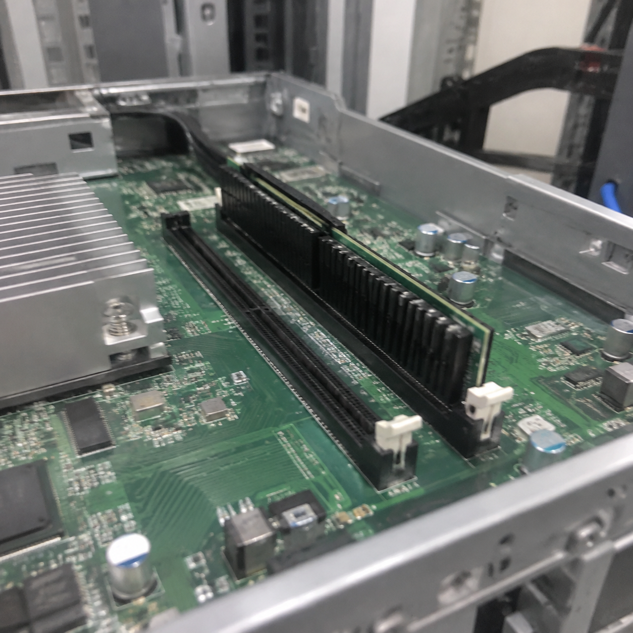
In my daily presales work with system integrators and hyperscale data center operators, memory specification mismatches remain a leading cause of deployment delays. RMA returns cost time and disrupt project rollouts. Let us examine the exact validation framework our engineering team uses to verify compatibility before issuing purchase orders.
Which architectural specs dictate whether your enterprise RAM is compatible?
Procurement teams often assume that purchasing higher-tier enterprise memory automatically guarantees backward or lateral platform support. In reality, inserting registered memory into a system designed strictly for unbuffered modules results in an immediate failure to complete POST. Navigating enterprise memory architecture requires a rigorous check against the integrated memory controller specifications.
Your server RAM is compatible only when the module architecture matches the exact physical and electrical signalling paths designed into the processor memory controller. You cannot mix or cross-install unbuffered (UDIMM), registered (RDIMM), or load-reduced (LRDIMM) modules within the same platform. Error-correcting code (ECC) and non-ECC variants are similarly mutually exclusive.
The Fundamental Boundaries: UDIMM vs. RDIMM vs. LRDIMM
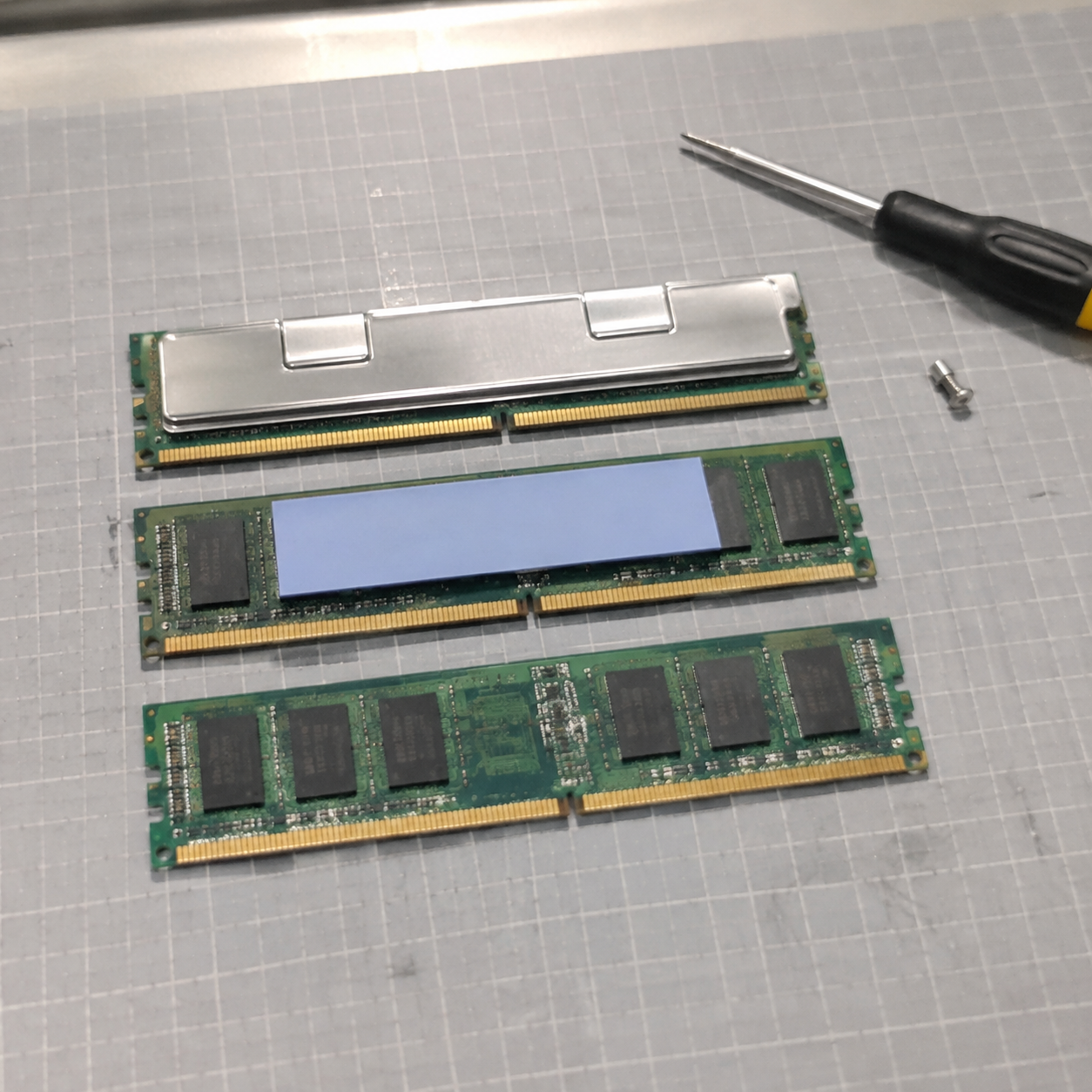
One of the most frequent RFQ revisions I handle involves tier mismatches between server classes. Enterprise platforms divide memory into three mutually incompatible structural tiers:
- Unbuffered DIMMs (UDIMMs): These modules connect memory chips directly to the CPU memory controller. They offer low latency for single-socket edge servers and workstations, but electrical load limits severely restrict total system density.
- Registered DIMMs (RDIMMs): These modules integrate a hardware register (a buffer) between the memory chips and the memory controller for address and command lines[^1]. This register stabilizes the electrical load, which allows platforms to run higher capacities and more modules per channel.
- Load-Reduced DIMMs (LRDIMMs): These modules buffer both command/address lines and data lines using a dedicated memory buffer chip[^2]. By presenting a single electrical load to the controller regardless of module density, they unlock extreme capacities at the cost of slight latency additions.
These technologies do not interoperate. If your motherboard manual and CPU specifications require RDIMMs, installing higher-density LRDIMMs or lower-cost UDIMMs will prevent the system from initializing memory training.
| Metric | UDIMM | RDIMM | LRDIMM |
|---|---|---|---|
| Buffering Level | None | Address and Command lines | Address, Command, and Data lines |
| Electrical Load on Controller | High per chip | Low (buffered register) | Lowest (full isolation buffer) |
| Maximum Capacity Scale | Low (typically up to 128GB/system) | High (typically up to 1TB–2TB/system) | Extreme (multi-terabyte environments) |
| Latency Penalty | Base (lowest) | ~1 clock cycle added | Additional buffer delay |
| Cross-Platform Interoperability | None (cannot mix with R/LR) | None (cannot mix with U/LR) | None (cannot mix with U/R) |
Error-Correcting Code (ECC) Mechanics
Enterprise platforms rely on ECC to detect and correct single-bit memory errors caused by electrical noise and cosmic radiation[^3]. An ECC module incorporates additional physical memory chips (an extra 8 bits per 64-bit bus width in traditional DDR4, or dedicated sub-channel metadata in DDR5[^4]) to calculate and verify parity data.
When vetting an upgrade, you must verify that the processor and motherboard chipset explicitly support ECC. While some entry-level processors physically accept ECC UDIMMs, consumer-grade desktop chipsets will silently disable ECC functionality or refuse to boot entirely. In mission-critical environments, running non-ECC memory introduces unacceptable operational risk.
Procurement Rule: Never assume higher specifications mean universal compatibility. Upgrading an edge node from UDIMMs to RDIMMs because "RDIMMs are enterprise-grade" will reliably render your node unbootable.
How do rank limits and channel topology ensure server RAM is compatible?
Many procurement managers verify generation and raw module speed, yet their systems still fail to boot or clock down unexpectedly after an upgrade. Memory controllers enforce strict electrical limits on total physical ranks per channel. Overloading your channel topology forces downclocking and invites intermittent bus crashes under peak throughput.
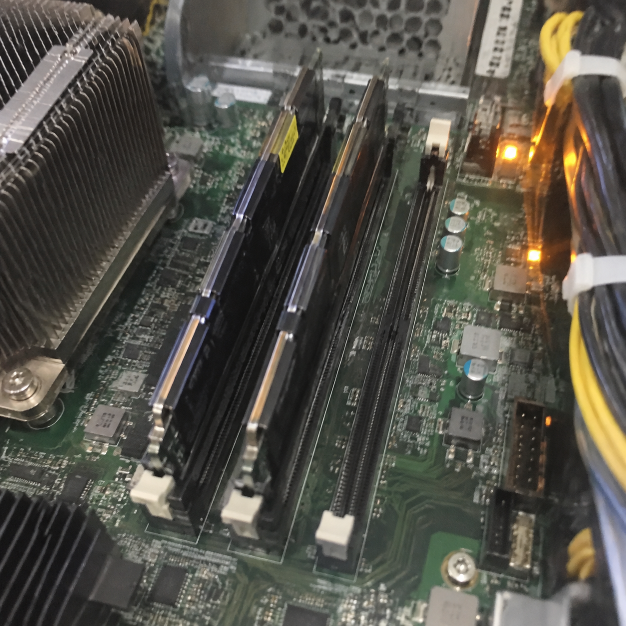
To ensure your server RAM is compatible, you must calculate total rank loading per memory channel alongside motherboard slot population rules. Processors support a fixed number of electrical ranks per channel. Exceeding rank budgets or populating slots in an arbitrary sequence triggers automatic downclocking, channel shutoff, or system halt errors.
Understanding Memory Ranks and Electrical Loading
A memory rank is a 64-bit data block (or 72-bit with ECC)[^5] created using some or all of the DRAM chips on a module. Modules come in single-rank (1R), dual-rank (2R), quad-rank (4R), and octal-rank (8R) configurations.
Your CPU memory controller does not count the physical sticks of RAM you install. Instead, it counts the total number of ranks connected to each memory channel:
- Direct Loading Limits: Most modern dual-socket enterprise processors support up to 8 memory channels per socket, with 1 or 2 DIMMs per channel (DPC). However, each channel can generally only handle a maximum of 8 physical ranks.
- The High-Density Trap: If you populate a 2-DPC channel with two quad-rank (4R) standard RDIMMs, you reach the electrical limit of the channel. Adding faster or denser standard modules beyond that will overload the memory controller bus.
- LRDIMM Rank Multiplication: Load-reduced modules circumvent this limit through rank multiplication. The buffer chip presents a physical quad-rank module to the controller as a logical dual-rank module[^6]. This design keeps the system within electrical boundaries while multiplying usable density.
The Reality of DIMMs Per Channel (DPC) Downclocking
Procurement teams often buy 3200 MT/s or 4800 MT/s modules and then discover their servers are operating at lower speeds in production. This reduction is rarely caused by faulty silicon. It is an intentional stability behavior defined by platform topology:
| Platform Configuration | DDR4 Rated Speed | Actual Operating Speed | DDR5 Rated Speed | Actual Operating Speed |
|---|---|---|---|---|
| 1 DIMM Per Channel (1 DPC) | 3200 MT/s | 3200 MT/s | 4800 MT/s | 4800 MT/s |
| 2 DIMMs Per Channel (2 DPC - 1R/2R) | 3200 MT/s | 2933 MT/s or 2666 MT/s | 4800 MT/s | 4000 MT/s or 3600 MT/s |
| 2 DIMMs Per Channel (2 DPC - 4R/8R) | 2933 MT/s | 2400 MT/s or 2133 MT/s | 4400 MT/s | 3200 MT/s |
CPU Socket
  ├── Memory Channel A
  │     ├── Slot 0 (White Tab)  --> Populate First  (Primary Load)
  │     └── Slot 1 (Black Tab)  --> Populate Second (Secondary Load)
  └── Memory Channel B
        ├── Slot 0 (White Tab)  --> Populate First
        └── Slot 1 (Black Tab)  --> Populate Second
I regularly review RFQs where clients request peak-rated frequencies while fully populating every physical slot on a dense 2-DPC motherboard. We must advise them that their actual throughput will automatically settle at lower speeds to maintain signal integrity across parallel traces.
Moving Beyond the Qualified Vendor List (QVL)
A motherboard manufacturer's Qualified Vendor List (QVL) is a valuable historical record of what the vendor physically tested in their lab before product launch. However, a QVL is never exhaustive. Memory manufacturers frequently update die revisions (e.g., Micron A-die to B-die, or Samsung B-die to C-die) without changing top-level model identifiers.
Instead of relying solely on exact module part numbers on a static QVL, verify compatibility through foundational parameters:
- DRAM component density (8Gb, 16Gb, or 32Gb monolithic dies).
- CAS latency (CL) and timing profiles compatible with platform JEDEC baselines.
- Voltage levels (e.g., standard 1.2V DDR4 vs. low-voltage 1.1V DDR5). Do not expect enterprise servers to support consumer overvolting profiles like XMP or EXPO.
How do firmware and physical form factors prove your RAM is compatible?
Packaging enterprise hardware into dense 1U rackmount enclosures or edge computing nodes introduces physical space limits and thermal risks. Even if memory timings match the CPU specifications on paper, modules can overheat or fail memory training without proper BIOS microcode. Real-world compatibility requires physical clearance, cooling verification, and firmware validation.
You confirm your server RAM is compatible by auditing module heights against chassis airflow guides, verifying thermal operating limits, and flashing BIOS revisions that support your target DRAM die densities. High-density enterprise enclosures often require specialized Very Low Profile (VLP) modules and up-to-date microcode to complete memory training during the power-on self-test.
Mechanical Clearances and Airflow Routing
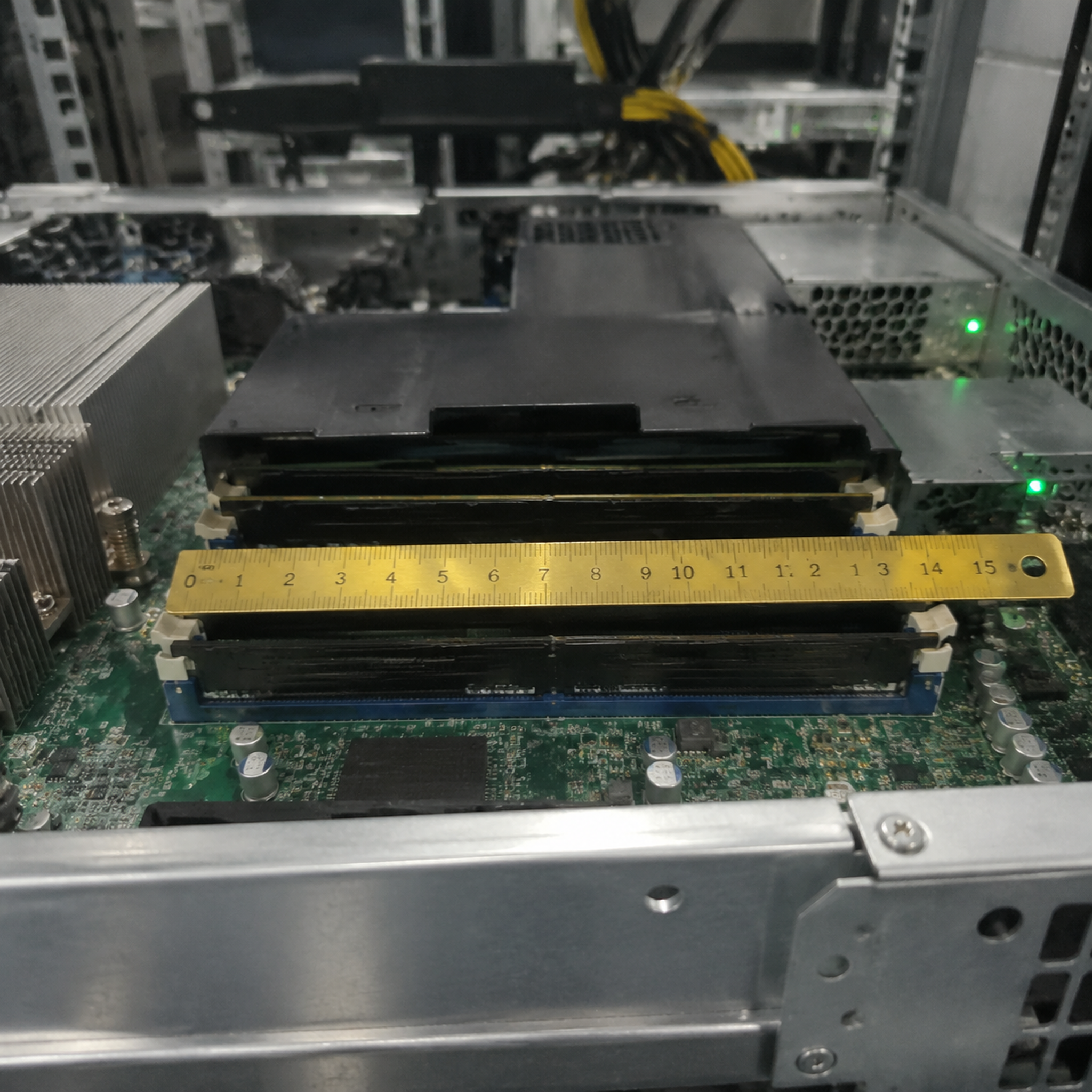
Standard enterprise DIMMs measure approximately 31.25 mm in height[^7]. While this height fits standard 2U to 4U chassis, specialized compute configurations create immediate physical clearance issues:
- 1U Blade and High-Density Servers: Angled or horizontal mezzanine slots in compact chassis frequently require Very Low Profile (VLP) modules measuring roughly 18.75 mm in height[^8]. Attempting to fit standard-height memory under an internal plastic air shroud will crush modules or block the chassis lid.
- Thermal Dissipation and Airflow Shadows: High-capacity RDIMMs and LRDIMMs integrate dense power management ICs (PMICs in DDR5)[^9] and dual-sided memory dies that run hot. In passive server cooling tunnels, modules positioned farthest from chassis fans sit in the thermal wake of forward modules. Unvalidated heat spreader additions can alter aerodynamic balance, causing thermal throttling under sustained write loads.
The Role of BIOS Revisions and Memory Training Microcode
System stability depends heavily on the firmware managing the physical hardware. Modern memory initialization involves an extensive "memory training" phase during POST. The CPU memory controller sends test signals to the memory chips to calibrate impedance, signal timing, and voltage margins across trace lines[^10].
Cold Boot Initiated
       │
       ▼
Read SPD EEPROM Chip via I2C/I3C Bus
       │
       ▼
Match Platform Microcode & DRAM Die Density
       ├── Failure ──> System Halts (No POST / BEEP Code)
       └── Success
             │
             ▼
Run Signal Training Algorithm (Impedance & Delay Calibration)
       ├── Marginal Signals ──> Memory Bus Downclocked
       └── Clean Signals    ──> Full Rated Operational Bus Speed
When new DRAM density nodes launch (such as 24Gb or 32Gb die revisions in DDR5 ecosystems[^11]), older motherboard firmware does not recognize the Serial Presence Detect (SPD) configurations. The server will hang at a black screen with memory initialization error codes.
Before signing off on bulk component orders for an existing server pool:
- Check BIOS Release Notes: Confirm that the target board firmware explicitly includes microcode updates for your target memory density and manufacturer die revision.
- Standardize Golden Images: Never deploy mixed-firmware boards across the same cluster when scaling memory. Inconsistent training algorithms can produce erratic latency variations across identical server nodes.
Frequently Asked Questions
Can I mix different RAM brands or speeds in the same server?
You can mix brands if the modules share identical voltage, rank structure, and timing profiles. The server will automatically downclock all memory to match the slowest module installed. However, mixing memory types (such as UDIMMs with RDIMMs) or mixing different memory densities across the same channel is not supported.
What happens if I install RDIMMs into a system that requires UDIMMs?
The system will fail to boot and will stop during the power-on self-test (POST). Entry-level processors and consumer-grade motherboards lack the physical wiring and memory controller logic required to drive the register clock chip on an RDIMM, resulting in a no-memory-detected hardware error.
Does a Qualified Vendor List (QVL) contain all compatible RAM options?
No. A QVL only lists the specific memory modules tested by the manufacturer before the product launched. Memory that matches the JEDEC standards, rank parameters, voltage, and architecture required by your platform's chipset and CPU will work, even if its exact part number does not appear on the QVL.
Why did my server downclock my memory frequency after an upgrade?
Your server downclocked because adding more modules increased the electrical load on the memory channels. Populating two DIMMs per channel (2 DPC) or using multi-rank modules increases signal reflections across motherboard traces[^12]. The memory controller lowers clock frequency to protect data integrity and prevent bus errors.
Conclusion
Confirming that your enterprise RAM is compatible requires an architectural approach. You must look past physical socket designs and surface-level DDR ratings. Safe procurement depends on cross-referencing your CPU memory controller limits, calculating channel rank budgets, respecting platform population rules, and auditing physical chassis clearances. Overlooking these structural dependencies leads to costly component returns and unexpected downtime.
If you are planning a large-scale server build or lifecycle hardware upgrade, let our engineering team validate your memory topology before you procure. Contact our technical sales department to submit your platform specifications for end-to-end component validation and OEM server manufacturing support.
[^1]: "Registered memory", https://en.wikipedia.org/wiki/Registered_memory. Standards from JEDEC Solid State Technology Association define Registered DIMM (RDIMM) architectures as incorporating a Registering Clock Driver (RCD) to buffer command and address busses while leaving data lines unbuffered. Evidence role: mechanism; source type: institution. Supports: RDIMMs utilize an onboard registering clock driver (RCD) to re-drive command, address, and clock signals, reducing capacitive load on the memory controller.. [^2]: "Twin-Load: Building a Scalable Memory System over ...", https://arxiv.org/html/1505.03476v1. JEDEC specifications for Load-Reduced DIMMs specify the inclusion of distributed or centralized data buffers (DB) alongside the register to fully isolate both data and control lines from the host channel. Evidence role: mechanism; source type: institution. Supports: LRDIMMs incorporate memory buffers or data buffers that isolate both data bus lines and command/address lines from the primary host memory bus.. [^3]: "Soft error", https://en.wikipedia.org/wiki/Soft_error. Empirical studies on semiconductor reliability demonstrate that energetic cosmic-ray neutrons and packaging alpha particles induce bit-flips in silicon memory cells without causing permanent hardware damage. Evidence role: mechanism; source type: paper. Supports: Atmospheric neutrons originating from cosmic radiation are a primary environmental mechanism causing soft errors and single-event upsets in semiconductor DRAM cells.. [^4]: "DDR5 SDRAM", https://en.wikipedia.org/wiki/DDR5_SDRAM. JEDEC standard JESD79-5 establishes that DDR5 DIMMs use two independent 32-bit sub-channels per module, with server variants expanding each sub-channel to 40 bits to accommodate sideband parity and error correction. Evidence role: definition; source type: institution. Supports: DDR5 splits each DIMM channel into two independent 32-bit sub-channels, each allocated additional metadata/parity bits (typically 8 bits per 32-bit data block on ECC modules).. [^5]: "Dynamic random-access memory", https://en.wikipedia.org/wiki/Dynamic_random-access_memory. Standard computer architecture definitions describe a memory rank as an independent block of DRAM chips configured to provide the full 64-bit data bus width, or 72 bits when including parity for error-correcting codes. Evidence role: definition; source type: education. Supports: A memory rank comprises a set of DRAM devices connected to the same chip select signal to create an undivided 64-bit data path (72-bit when incorporating ECC check bits).. [^6]: "PfHP Matrix-matrix multiplication via rank-1 updates", https://www.cs.utexas.edu/~flame/laff/pfhp/week1-mmmult-via-rank-1.html. Technical analyses of enterprise memory subsystems document how LRDIMM buffer controllers translate physical multi-rank DRAM arrangements into fewer logical ranks, mitigating electrical bus loading limits. Evidence role: mechanism; source type: research. Supports: LRDIMM buffer logic performs rank multiplication, virtualizing multiple physical ranks into fewer logical ranks visible to the host memory controller.. [^7]: "DIMMs", https://en.wikipedia.org/wiki/DIMM. JEDEC standard mechanical outlines (such as MO-309 and MO-329) define the baseline height of standard DDR4 and DDR5 enterprise DIMM printed circuit boards as 31.25 mm. Evidence role: definition; source type: institution. Supports: Standard JEDEC memory module form factor outlines specify a nominal board height of 31.25 mm.. [^8]: "DIMMs", https://en.wikipedia.org/wiki/DIMM. JEDEC packaging specifications define the Very Low Profile (VLP) form factor with a maximum component height of 18.75 mm to permit horizontal and dense vertical placement in 1U blade enclosures. Evidence role: definition; source type: institution. Supports: VLP (Very Low Profile) memory modules conform to an industry standard maximum height of approximately 18.75 mm.. [^9]: "DDR5 SDRAM", https://en.wikipedia.org/wiki/DDR5_SDRAM. Under JEDEC DDR5 specifications, voltage regulation is transferred from the motherboard directly onto the memory module via an integrated PMIC, delivering tighter voltage tolerances and granular power telemetry. Evidence role: mechanism; source type: institution. Supports: DDR5 standardizes the integration of local Power Management ICs (PMICs) directly onto the DIMM substrate rather than relying solely on host motherboard voltage regulators.. [^10]: "High speed DRAM transceiver design for low voltage ...", https://repository.library.northeastern.edu/files/neu:cj82pn106/fulltext.pdf. Studies on high-speed DRAM bus initialization describe the memory training sequence as an iterative calibration of on-die termination (ODT), receiver voltage reference (Vref) levels, and per-pin read/write timing delays. Evidence role: mechanism; source type: paper. Supports: Memory training algorithms executed by the host firmware calibrate drive strength, on-die termination impedance, trace timing skews, and voltage thresholds.. [^11]: "DDR5 SDRAM", https://en.wikipedia.org/wiki/DDR5_SDRAM. Updates to the JEDEC DDR5 SDRAM standard (JESD79-5) formally added support for 24Gb non-binary monolithic dies, enabling non-power-of-two memory module capacities such as 24GB, 48GB, and 96GB. Evidence role: definition; source type: institution. Supports: The JEDEC DDR5 specification formalized intermediate 'non-binary' DRAM component densities, including 24Gb monolithic dies.. [^12]: "Model predictive control design for load frequency control ...", https://researchrepository.wvu.edu/cgi/viewcontent.cgi?article=2816&context=etd. High-speed transmission line analyses demonstrate that populating multiple DIMMs on a single channel introduces secondary stub reflections and inter-symbol interference, requiring downclocking to maintain valid signal timing margins. Evidence role: mechanism; source type: paper. Supports: Attaching multiple DIMMs per channel creates trace stubs and capacitive loading that degrade eye diagrams via transmission line reflections, necessitating lower clock frequencies..
发表回复