

Enterprise buyers often ask if they can mix DDR4 and DD […]
Enterprise buyers often ask if they can mix DDR4 and DDR5 RAM to stretch IT refresh budgets, but doing so creates severe system failures. Incompatible memory platforms stop server deployments in their tracks, risking costly project milestones and vendor disputes. Hardware integration requires strict adherence to architectural boundaries to protect your infrastructure investment.
No, it is not okay to mix DDR4 and DDR5 RAM in any system. DDR4 and DDR5 modules are physically, electrically, and architecturally incompatible. They feature distinct key notch locations, different pin assignments, and fundamentally opposing voltage architectures. A system can run either DDR4 or DDR5 memory, but never both technologies simultaneously.
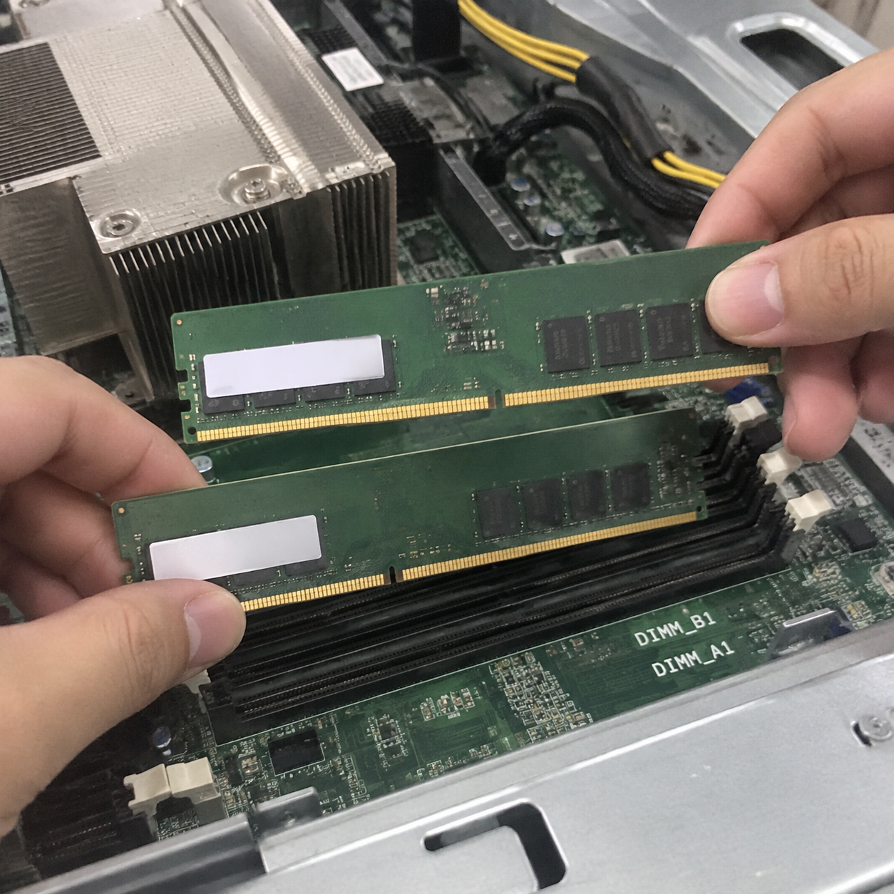
Hardware teams often assume hybrid memory configurations are feasible after reviewing multi-generation processor specifications. I have mediated several tense technical procurement meetings where this assumption caused expensive project roadblocks. Let us examine the technical realities, architectural boundaries, and procurement practices that govern modern memory deployment.
Why is it electrically impossible to mix DDR4 and DDR5 RAM?
Hardware engineers face catastrophic motherboard damage when procurement teams force unsupported memory combinations onto deployment benches. Misunderstanding internal power rails creates high component attrition, blown circuits, and prolonged downtime across enterprise server lines. Sourcing teams must recognize the immutable physics that dictate modern enterprise memory standards before issuing purchase orders.
You cannot electrically mix DDR4 and DDR5 RAM because DDR5 moves voltage regulation directly onto the memory module itself. While DDR4 relies on the motherboard voltage regulator module (VRM) for 1.2V power, DDR5 uses an onboard Power Management Integrated Circuit (PMIC) operating at a 1.1V baseline[^1].
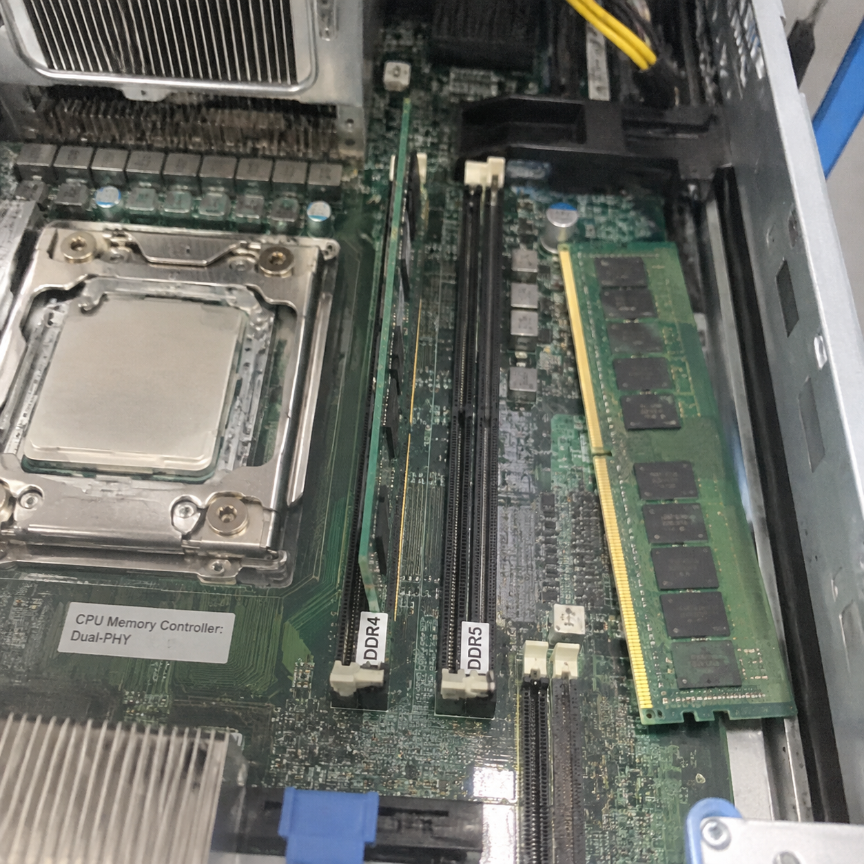
Physical Pinouts and Mechanical Keying
DDR4 and DDR5 DIMMs both feature 288 pins[^2], yet their pin definitions share almost nothing in common. The engineering consortium JEDEC deliberately shifted the mechanical key notch toward the center on DDR5 modules[^3]. This design choice prevents a technician from seating a DDR5 module into a DDR4 slot, or vice versa.
Forcing a DIMM into an incompatible socket will crack the printed circuit board (PCB) traces or crush the socket gold fingers. During a factory audit last quarter, I inspected two failed server prototypes where contract assemblers attempted to bypass alignment keys on custom backplanes. Both motherboards were completely ruined before ever passing post-manufacturing power-on self-tests.
DDR4 DIMM:  [====== Notch closer to edge ======] (1.2V Motherboard VRM)
DDR5 DIMM:  [======== Notch closer to center ========] (1.1V On-Module PMIC)
The Architectural Shift to On-Module PMICs
The electrical divide between these two memory generations runs far deeper than mechanical pin arrangements. DDR4 memory relies entirely on motherboard circuitry to step down standard system power to 1.2V. The motherboard handles transient voltage spikes, rail switching, and thermal throttling for every populated DDR4 channel.
DDR5 revolutionizes enterprise power architecture by relocating the PMIC directly onto the memory module substrate. The motherboard feeds an unmanaged 12V rail straight to the DDR5 DIMM[^4]. The onboard PMIC then downconverts this feed to 1.1V for standard VDD and VDDQ planes, while generating auxiliary 1.8V rails for peripheral logic[^5].
| Technical Specification | DDR4 Architecture | DDR5 Architecture | System Impact |
|---|---|---|---|
| Operating Voltage (VDD/VDDQ) | 1.2V standard | 1.1V standard | Lower baseline energy draw on DDR5 |
| Voltage Regulation | Motherboard-based VRM | On-DIMM PMIC | DDR5 isolates rail noise per module |
| Pin Configuration | 288 pins (Legacy layout) | 288 pins (Redesigned routing) | Modules cannot fit alternate sockets |
| Channel Architecture | 1 x 72-bit channel (with ECC) | 2 x 40-bit subchannels (with ECC)[^6] | DDR5 improves memory bus concurrency |
| On-Die Error Correction | None (Relies on Sideband) | Native On-Die ECC[^7] | DDR5 corrects cell faults internally |
Because of this radical electrical departure, a unified power bus cannot coexist on a single memory trace. Feeding a 12V unmanaged power rail into a legacy DDR4 memory interface would immediately destroy the DRAM silicon.
Why do hybrid processor architectures trick buyers into trying to mix DDR4 and DDR5 RAM?
Procurement teams frequently misread hybrid processor specifications and assume their future platforms can handle mixed memory types. Sourcing specialists order balanced quantities of both generations, expecting flexibility during component shortages, only to encounter total system incompatibility. Clarifying processor capabilities versus motherboard execution protects your supply chain from costly restocking penalties.
Hybrid processor architectures mislead buyers because the central processing unit (CPU) memory controller contains physical physical-layer (PHY) interfaces for both standards. However, the processor can only initialize one memory protocol per boot sequence. A motherboard routed for one standard cannot communicate with or operate the other standard concurrently.
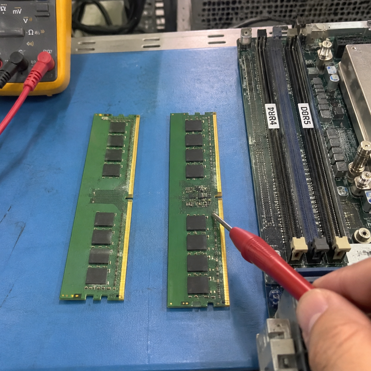
The Dual-PHY Memory Controller Reality
Modern server and enterprise edge processors, such as Intel 12th through 14th Gen Core architectures and select embedded platforms, maintain broad memory support. Their integrated memory controllers incorporate dual-mode physical-layer routing[^8]. This silicon design allows tier-one original equipment manufacturers (OEMs) to engineer either DDR4 or DDR5 system platforms around a single CPU socket.
Procurement departments see "DDR4 and DDR5 support" printed on enterprise processor spec sheets and infer that operational flexibility extends to the slot level. That conclusion is incorrect. The processor microcode detects the active memory type during system initialization and switches its internal timing state machines to match that standard exclusively. It cannot split memory controller channels between disparate clock frequencies, timing registers, and bus command structures.
The Myth of the "Combo" Motherboard
Buyers occasionally cite consumer-grade "combo motherboards" from overseas distributors as evidence that memory mixing works. These niche platforms usually feature two DDR4 slots alongside two DDR5 slots. Non-technical buyers view these boards as an ideal hedge against fluctuating memory costs during multi-rack data center rollouts.
Every combo board on the market comes with severe operating constraints:
- Mutual exclusivity is absolute: You can populate DDR4 slots, or you can populate DDR5 slots, but populating both causes an instant failure to boot.
- Severe signal integrity loss: Splitting high-frequency printed traces between four physical slots creates trace stubs. These stubs reflect electrical signals, degrade eye diagrams, and limit maximum memory speeds[^9].
- Zero enterprise validation: Tier-one server OEMs and server motherboard manufacturers never produce dual-socket or quad-channel enterprise platforms with split DIMM formats.
Relying on split-standard platforms in mission-critical environments introduces immense instability. I regularly steer enterprise clients away from these transitional gimmicks because they violate industrial uptime standards.
What operational risks arise when sourcing strategies attempt to mix DDR4 and DDR5 RAM?
Purchasing departments face severe operational gridlock when sourcing strategies attempt to mix DDR4 and DDR5 RAM across identical server platforms. Field service calls multiply, delivery schedules slip, and inventory reserves split into redundant, incompatible parts pools. Enterprise reliability depends on clean component standardization, comprehensive qualification, and disciplined lifecycle management across your fleet.
Attempting to mix generations across unified server deployments invalidates OEM platform warranties and destabilizes high-speed multi-channel memory busses. When mixed modules disrupt bus timings, servers encounter silent data corruption, kernel panics, and spontaneous reboots. These failures halt automated production lines and consume hundreds of engineering hours in root-cause isolation.
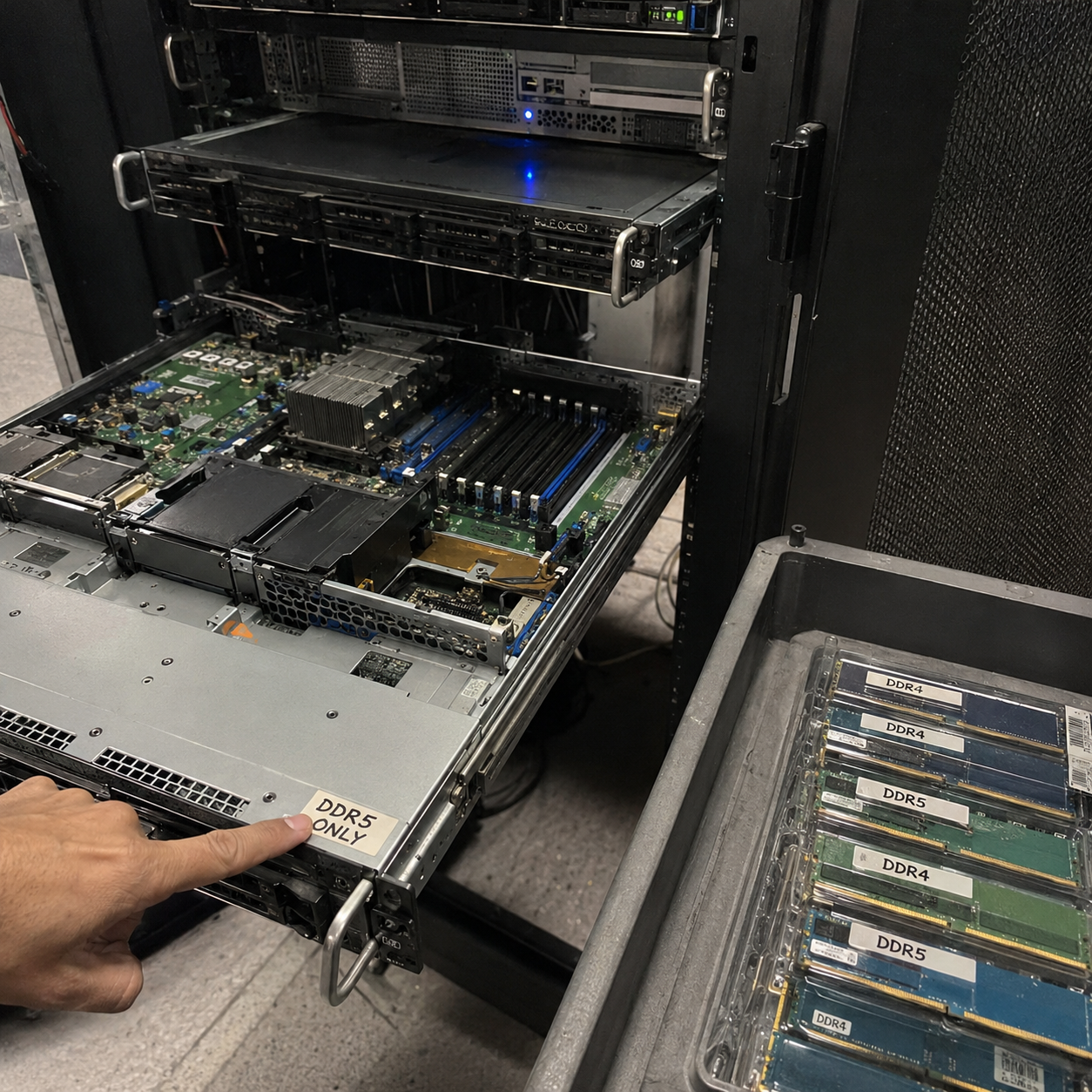
Signal Degradation and Multi-Channel Imbalance
Enterprise computing depends on balanced channel populates to maximize memory bandwidth. Modern dual-socket servers utilize six or eight memory channels per socket, with up to two DIMMs per channel (2DPC)[^10]. The system memory bus operates at frequencies measured in billions of transfers per second.
At these ultra-high frequencies, trace impedance and signal reflection margins are microscopic. Attempting to balance differing memory generations disrupts channel interleaving:
- Latency anomalies: DDR4 operates at lower baseline latencies (e.g., CL16 to CL22), while DDR5 operates at higher nominal latencies (e.g., CL36 to CL40)[^11] offset by raw clock speed. A system controller cannot arbitrate these conflicting timing windows.
- Subchannel mismatch: DDR5 splits the standard 64-bit data bus into two independent 32-bit subchannels per DIMM[^12]. DDR4 maintains a monolithic 64-bit data bus. The memory controller cannot bridge these transmission formats on a shared plane.
- Channel bandwidth starvation: If one memory channel lags behind another, CPU compute cores stall while waiting for cache refills. The resulting performance penalties eliminate any perceived cost savings from using leftover DDR4 inventory.
Enterprise Procurement Bottlenecks
In the OEM/ODM manufacturing space, standardizing memory kits is fundamental to preserving operational margins. When buying groups try to hedge supply chain delays by purchasing mixed lots of DDR4 and DDR5 systems without distinct SKU tracking, deployment errors explode.
Procurement Misstep:
[Mixed Generation Purchase Orders]
            │
            ▼
[Assembly Line Sorting Bottlenecks]
            │
            ▼
[Unmatched DIMM Installation Failures]
            │
            ▼
[High RMA Rates & Field Replacements]
A field replacement unit (FRU) strategy requires predictable parts availability. If your data center infrastructure contains haphazardly deployed DDR4 and DDR5 motherboards under identical chassis covers, field technicians will inevitably carry the wrong replacement DIMMs. The resulting maintenance delays compound system downtime and drive up service level agreement (SLA) penalties.
Operational Insight: Enterprise reliability is built on predictability. Always procure matched memory kits from an approved vendor list (AVL). Verify that all system motherboards within a single compute cluster share identical memory generation support, voltage profiles, and speed ratings.
Frequently Asked Questions
Can you put a DDR4 RAM stick into a DDR5 slot?
No, you cannot insert a DDR4 stick into a DDR5 slot. The physical notch on a DDR4 module sits in a different location than the notch on a DDR5 slot. Forcing the module into the socket will break the connector pins, fracture the motherboard PCB, and void your hardware warranty.
Why do some motherboards feature both DDR4 and DDR5 slots?
A few consumer and niche industrial motherboards feature both slot formats to offer upgrade flexibility. However, these systems only allow you to use one memory standard at a time. The motherboard will fail to post if you populate DDR4 and DDR5 slots simultaneously.
Can a BIOS update allow DDR4 and DDR5 to run together?
No, a BIOS update cannot enable DDR4 and DDR5 to operate concurrently. The barrier is physical and electrical, not firmware-based. The processor memory controller cannot supply different voltages or manage fundamentally opposing channel architectures across the same system bus.
Is DDR5 backwards compatible with DDR4 memory?
DDR5 is not backwards compatible with DDR4 memory modules. DDR5 memory features a redesigned 2x32-bit channel structure, native on-die error correction, and an onboard power management integrated circuit. These advancements require dedicated motherboard traces and a compatible processor memory controller.
Conclusion
System integrators and procurement teams cannot mix DDR4 and DDR5 RAM under any operational circumstances. Physical notch placement, conflicting voltage requirements, and completely different power architectures make simultaneous deployment impossible. Attempting to bridge memory generations inside a single platform risks physical equipment destruction, erratic data corruption, and catastrophic hardware downtime. Enterprise IT leaders must evaluate memory transitions at the full system architecture level, rather than treating memory as an incremental upgrade. If you are planning an enterprise server rollout, edge computing refresh, or high-density rack deployment, our engineering group can assist you. Contact our OEM/ODM technical team today to configure validated, carrier-grade server hardware tailored to your performance and reliability requirements.
[^1]: "DDR5 SDRAM", https://en.wikipedia.org/wiki/DDR5_SDRAM. Documented in JEDEC standard specifications JESD79-4 and JESD79-5, which define the operating voltage reduction from 1.2V to 1.1V and establish the on-DIMM PMIC architecture for DDR5. Evidence role: mechanism; source type: institution. Supports: DDR4 and DDR5 memory voltage regulation architectures and operating voltage baselines. [^2]: "DDR5 SDRAM", https://en.wikipedia.org/wiki/DDR5_SDRAM. JEDEC standard module outlines specify a 288-pin edge connector for both standard DDR4 and DDR5 dual in-line memory modules. Evidence role: definition; source type: encyclopedia. Supports: DDR4 and DDR5 standard UDIMM/RDIMM pin count specification. Scope note: Pin count refers to standard desktop and server DIMMs; small-outline SODIMM form factors employ different pin counts. [^3]: "DIMMs", https://en.wikipedia.org/wiki/DIMM. Outlined in JEDEC design standard publication MO-329, which details the modified key notch offset to prevent mechanical mating with legacy DDR4 sockets. Evidence role: mechanism; source type: institution. Supports: Alteration of the mechanical key notch position between DDR4 and DDR5 modules. [^4]: "Rambus Expands Chipset for Advanced Data Center Memory ...", https://investor.rambus.com/press-releases/press-release-details/2024/Rambus-Expands-Chipset-for-Advanced-Data-Center-Memory-Modules-with-DDR5-Server-PMICs/default.aspx. Supported by JEDEC server PMIC standards (JESD301-1), which designate a 12V nominal input supply rail for enterprise RDIMM architectures. Evidence role: mechanism; source type: research. Supports: The 12V power distribution topology routed to the DDR5 RDIMM PMIC. Scope note: Client unbuffered DIMMs (UDIMMs) typically utilize a 5V input rail rather than the 12V rail specified for enterprise registered modules. [^5]: "Understanding PMIC, SPD Hub, and the 1.1V VDD Rail", https://www.reddit.com/r/LaptopRepairEngineer/comments/1sxmtsp/ddr5_no_post_understanding_pmic_spd_hub_and_the/. Detailed in JEDEC standard JESD79-5, specifying that the module PMIC supplies the core voltages alongside a secondary 1.8V VPP wordline boost supply. Evidence role: mechanism; source type: institution. Supports: On-module generation of auxiliary 1.8V VPP rails in DDR5 memory. [^6]: "DDR5 SDRAM", https://en.wikipedia.org/wiki/DDR5_SDRAM. Documented in JEDEC architectural briefings for DDR5, which define the transition from a single 72-bit channel to two independent 40-bit subchannels (32 data bits plus 8 ECC/sideband bits). Evidence role: mechanism; source type: research. Supports: DDR5 channel topology comprising two independent 40-bit subchannels for ECC RDIMMs. [^7]: "ECC memory", https://en.wikipedia.org/wiki/ECC_memory. Described in IEEE transactions on memory systems and JEDEC JESD79-5, detailing internal Hamming code circuitry designed to correct single-bit errors within dense DRAM silicon nodes. Evidence role: mechanism; source type: paper. Supports: Integration of on-die error-correcting code in standard DDR5 DRAM dies. Scope note: On-die ECC operates within the individual DRAM chips and does not replace channel-level transport ECC used in enterprise servers. [^8]: "Tried 128GB DDR5 on 12th gen Alder Lake", https://www.reddit.com/r/intel/comments/uqcn00/tried_128gb_ddr5_on_12th_gen_alder_lake_it/. Documented in Intel architecture white papers for 12th–14th Generation Core processors, which describe a reconfigurable PHY capable of operating in either DDR4 or DDR5 mode on mutually exclusive board layouts. Evidence role: mechanism; source type: paper. Supports: Processor memory controllers implementing dual-mode PHYs for DDR4 and DDR5 support. [^9]: "An End-to-End Design and Simulation Methodology for ... - PMC", https://pmc.ncbi.nlm.nih.gov/articles/PMC12943540/. Corroborated by standard electrical engineering texts on high-speed digital design, showing that unterminated transmission line stubs generate impedance discontinuities and signal reflections that collapse receiver eye margins. Evidence role: mechanism; source type: education. Supports: Signal integrity degradation and impedance mismatches induced by printed trace stubs. [^10]: "Multi-channel memory architecture", https://en.wikipedia.org/wiki/Multi-channel_memory_architecture. Reflected in platform architectural briefs for modern x86 server families (such as Intel 4th/5th Gen Xeon Scalable and AMD EPYC 7003/9004 series), which specify 8 to 12 memory channels per socket supporting 1DPC and 2DPC topologies. Evidence role: general_support; source type: institution. Supports: Multi-channel memory architecture standards in modern enterprise server processors. Scope note: Exact channel count varies by generation and processor tier, ranging from 6 to 12 channels per socket. [^11]: "DDR4 SDRAM", https://en.wikipedia.org/wiki/DDR4_SDRAM. Specified in JEDEC JESD79-4 and JESD79-5 timing standard tables, indicating baseline speed bins and corresponding CAS latency parameters. Evidence role: statistic; source type: institution. Supports: Standard JEDEC CAS latency ranges across DDR4 and DDR5 memory modules. Scope note: Absolute nanosecond latency remains roughly equivalent because higher nominal clock frequencies offset the increased cycle count of DDR5. [^12]: "DDR5 SDRAM", https://en.wikipedia.org/wiki/DDR5_SDRAM. Defined in JEDEC JESD79-5, detailing the structural reorganization of the traditional 64-bit bus into two independent 32-bit subchannels with dedicated command and address lines. Evidence role: mechanism; source type: institution. Supports: Subchannel subdivision of the 64-bit memory data bus in DDR5.
发表回复