

Evaluating RAM compatibility across enterprise compute […]
Evaluating RAM compatibility across enterprise compute platforms can quickly turn into a logistical nightmare for procurement teams. A module might fit into a motherboard slot, yet it can still trigger silent POST failures, disabled memory channels, or system instability during deployment. In this guide, I break down the architectural and electrical variables you must evaluate before issuing a purchase order.
No, RAM is not compatible with everything because system memory depends on strict physical, architectural, and electrical tolerances. Memory modules must match the motherboard generation, processor memory controller limits, voltage requirements, and module topology. Even when a stick physically fits into a slot, mismatched ranks, timings, or unsupported buffer types will cause boot failures or severe performance degradation.
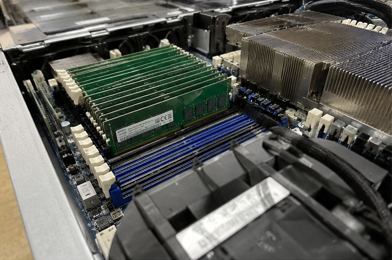
In my pre-sales consultations with system integrators, memory mismatches represent one of the most frequent causes of delayed server rollouts. Many buyers assume that DRAM functions as a universal plug-and-play component. Let us examine the technical layers that govern true compatibility across enterprise systems.
Does physical slot fit guarantee RAM compatibility?
Procurement teams often assume that if a memory module seats securely into a DIMM slot, the installation will succeed. That false assumption leads to damaged connector pins, blown traces, and costly component returns. You must understand physical tolerances before you evaluate electrical behavior.
Physical insertion into a motherboard slot does not ensure RAM compatibility. While keyed notches prevent mixing DDR generations like DDR4 and DDR5, form factors such as standard DIMMs, SO-DIMMs, and low-profile variants carry different pinout configurations and voltage mappings. Physical seating is only a mechanical prerequisite, not an indicator of operational compatibility.
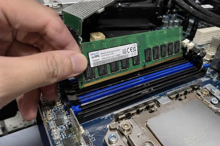
Mechanical Keying Across JEDEC Generations
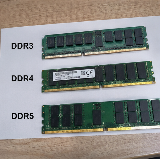
Every generation of Double Data Rate (DDR) synchronous dynamic random-access memory follows strict JEDEC standards. JEDEC changes the pin count and the location of the mechanical key notch for every generation[^1]. This physical notch prevents engineers from accidentally inserting a DDR4 module into a DDR5 socket.
DDR4 modules utilize 288 pins with a curved edge connector to reduce insertion force[^2]. DDR5 modules also feature 288 pins, but the alignment notch sits closer to the center. If an installer applies excessive pressure to force a mismatched module into a board, the socket will crack and the gold trace fingers will shear off.
| Memory Generation | Pin Count | Standard Operating Voltage | Key Notch Position | On-Module Power Management |
|---|---|---|---|---|
| DDR3 | 240 | 1.5V / 1.35V (DDR3L) | Off-center left | No (Motherboard VRM) |
| DDR4 | 288 | 1.2V | Off-center right | No (Motherboard VRM) |
| DDR5 | 288 | 1.1V | Near center | Yes (Onboard PMIC) |
Form Factor and Thermal Clearance Restraints
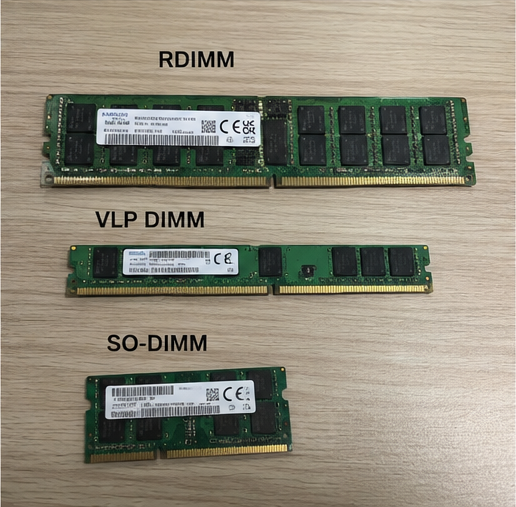
Even within the same generation, form factors vary significantly:
- Standard Registered DIMMs (RDIMMs): Standard height modules used in traditional 2U to 4U rackmount servers.
- Very Low Profile (VLP) DIMMs: Engineered for 1U blade servers and high-density compute nodes where vertical clearance is limited.
- Small Outline DIMMs (SO-DIMMs): Built with 260 pins (DDR4) or 262 pins (DDR5)[^3] for compact industrial PCs and edge appliances.
In a recent consultation, a client procured standard-profile modules for an ultra-dense 1U edge compute chassis. While the modules matched the motherboard chipset, their physical height obstructed the internal cooling shroud. The system could not close, and the thermal path was completely compromised. Physical compatibility requires verifying module height, latch clearance, and chassis airflow design.
How do CPU and chipset limits affect RAM compatibility?
Hardware buyers frequently procure high-frequency memory only to discover their servers downclock to baseline speeds or fail to boot entirely. Neglecting the processor memory controller causes silent throughput bottlenecks. To protect your hardware investment, you must evaluate the silicon limits upstream.
CPU memory controllers and motherboard chipsets dictate enterprise RAM compatibility by setting hard limits on maximum operational frequency, total addressable capacity, and channel population rules. If you populate all channels across multiple ranks, the integrated memory controller often forces a lower operating frequency to maintain signal stability across high trace loads.
The Role of the Integrated Memory Controller (IMC)
Modern compute platforms no longer rely on legacy motherboard Northbridge chips to coordinate memory access. The Integrated Memory Controller (IMC) resides directly on the CPU die[^4]. Because the IMC handles all electrical signal lines to the memory buses, the CPU architecture dictates the speed ceiling.
For example, an enterprise motherboard may advertise support for DDR5 up to 5600 MT/s. However, if you install an entry-level server processor whose IMC only supports 4800 MT/s, the entire memory subsystem defaults to 4800 MT/s. The system does not break, but your procurement budget is wasted on unused frequency headroom.
DIMMs Per Channel (DPC) and Speed Degradation
Enterprise platforms utilize multi-channel memory layouts, ranging from 4-channel to 12-channel architectures per CPU socket. Each channel can host one or two DIMM slots. Populating multiple DIMMs per channel (DPC) introduces significant capacitive loading on the memory bus.
To maintain clean electrical signal margins, the processor IMC reduces operational frequency as more slots are filled[^5]:
- 1 DIMM Per Channel (1DPC): The memory bus runs at peak rated speed (e.g., 4800 MT/s or 5600 MT/s).
- 2 DIMMs Per Channel (2DPC): The electrical bus experiences higher trace impedance. The system automatically steps the frequency down (e.g., from 4800 MT/s down to 4400 MT/s or 4000 MT/s).
[ CPU Socket ]
      │
      ├── Memory Channel A ──► [ Slot 1 (Primary) ]   <-- 1DPC: Runs at Maximum Frequency
      │                    └──► [ Slot 2 (Secondary) ] <-- 2DPC: Triggers Speed Step-Down
      │
      └── Memory Channel B ──► [ Slot 1 (Primary) ]
                           └──► [ Slot 2 (Secondary) ]
When buyers do not account for rank multiplication, systems suffer unpredicted latency penalties. Quad-rank and octal-rank modules draw heavy current, forcing system administrators to choose between memory density and memory bandwidth.
Can you mix ECC and non-ECC memory types safely?
Warehouse inventory shortages often tempt engineers to mix available memory modules across identical server chassis. Combining fundamentally incompatible memory architectures triggers immediate POST halts and corrupted data pipelines. Knowing module classification boundaries prevents these integration disasters.
You cannot mix ECC and non-ECC memory types on the same platform or channel. Enterprise motherboards require specific memory buffers, meaning Registered DIMMs (RDIMMs), Load-Reduced DIMMs (LRDIMMs), and Unbuffered DIMMs (UDIMMs) cannot function together. Mixing these disparate architectures halts system boot sequences and causes immediate platform rejection.
Memory Module Classifications Explained
Enterprise hardware categorizes RAM based on error correction and command signal buffering:
- Non-ECC Unbuffered (UDIMM): Standard consumer memory without data-bus parity or register buffers.
- ECC Unbuffered (ECC UDIMM): Contains an extra DRAM chip per rank to detect and correct single-bit errors[^6], but command signals route directly to the CPU.
- ECC Registered (RDIMM): Features an onboard register chip that buffers command and address lines, reducing electrical loading on the memory controller[^7].
- Load-Reduced (LRDIMM): Buffers both command lines and data lines using a dedicated memory buffer chip[^8], allowing massive rank densities.
UDIMM:   [CPU Memory Controller] ═══════════════════════════► [DRAM Chips]
                                  (Direct connection creates high bus load)

RDIMM:   [CPU Memory Controller] ───► [Register Buffer] ────► [DRAM Chips]
                                  (Buffered command lines stabilize signal)

LRDIMM:  [CPU Memory Controller] ───► [Data & Buffer Hub] ──► [DRAM Chips]
                                  (Fully buffered for maximum capacities)
The Mechanism of POST Rejections
I regularly review inquiries from system builders who attempt to install standard consumer UDIMMs into dual-socket enterprise server boards. Because the enterprise chipset microcode explicitly expects communication with an RDIMM register clock driver, the system hangs at the Power-On Self-Test (POST) phase with an unrecoverable memory initialization error.
| Memory Type | Command Buffer | Data Buffer | Parity Check (ECC) | Platform Intermixability |
|---|---|---|---|---|
| UDIMM | None | None | No | Must run isolated; cannot mix |
| ECC UDIMM | None | None | Yes | Must run isolated; cannot mix |
| RDIMM | Yes (RCD) | None | Yes | Must run isolated; cannot mix |
| LRDIMM | Yes (RCD) | Yes (Data Buffers) | Yes | Must run isolated; cannot mix |
Even if an enterprise board supports both UDIMMs and RDIMMs (a rare feature limited to select single-socket workstations), you can never install both types simultaneously. The motherboard will disable the mismatched channel immediately.
Why does QVL validation determine enterprise RAM compatibility?
Relying solely on paper specifications creates severe operational vulnerabilities when scaling server infrastructure. Systems can pass initial staging, only to suffer random memory parity errors under enterprise production loads. Rigorous Qualified Vendor Lists (QVL) ensure long-term operational resilience.
Qualified Vendor Lists determine enterprise RAM compatibility by verifying that a specific memory module passed multi-corner electrical, thermal, and signal integrity testing[^9] on that exact board. A module meeting generic speed and density specs can still fail if its printed circuit board revision or DRAM die revision causes timing drift under load.
Beyond the JEDEC Standard: Die Steppings and SPD Profiles
Two memory modules can share identical high-level specifications: DDR4-3200, CL22, 1.2V, 32GB RDIMM. However, underneath the heat spreader, one vendor might use Samsung B-die components while another uses Micron E-die or SK Hynix A-die components.
Each silicon manufacturer implements slightly different sub-timings, capacitive behaviors, and drive-strength tolerances:
- Serial Presence Detect (SPD) Data: The BIOS reads timing profiles directly from an EEPROM chip on the module[^10]. If the motherboard microcode lacks an optimized profile for that specific die stepping, it applies loose, conservative sub-timings.
- Intermittent Timing Drift: Unvalidated modules frequently suffer from signal jitter when ambient temperatures rise inside high-density 1U chassis.
- Cold Boot and Reset Failures: Systems using unverified memory can run smoothly for weeks, but then fail to train the memory bus during a routine firmware reboot.
The Procurement Evaluation Framework
To eliminate risks during large-scale procurement, our OEM/ODM engineering teams advise buyers to follow a strict validation workflow:
- Cross-Reference Board QVL: Confirm that the exact manufacturer part number (including the revision suffix) appears on the platform QVL.
- Lock the Bill of Materials (BOM): Require your memory supplier to provide fixed-BOM guarantees so they do not swap DRAM dies between production batches.
- Verify Voltage Tolerances: Ensure that the platform power delivery system matches module voltage limits, especially with DDR5 onboard Power Management ICs (PMICs).
- Execute Burn-In Qualification: Run synthetic stress tests across fully populated memory channels for at least 72 hours before production deployment.
Frequently Asked Questions
Can DDR4 RAM fit into a DDR5 slot?
No, DDR4 RAM cannot fit into a DDR5 motherboard slot. JEDEC shifted the mechanical alignment notch on DDR5 modules toward the center of the edge connector. In addition, DDR5 operates at 1.1V with an onboard PMIC[^11], whereas DDR4 requires 1.2V supplied directly by the motherboard power plane.
What happens if you install faster RAM than your CPU supports?
If you install faster RAM than your processor supports, the system will automatically downclock the memory to match the maximum speed supported by the CPU memory controller. The hardware will operate safely, but you will not realize the extra speed you paid for.
Can you mix different RAM brands and densities in the same server?
You should never mix different RAM brands, capacities, or rank structures within the same memory channel. While a system might complete the boot cycle, mismatched module timings and drive strengths trigger channel de-synchronization, random operating system crashes, and silent data corruption[^12] under heavy memory workloads.
Why does a server fail to boot after adding more RAM?
A server usually fails to boot after adding memory due to exceeding maximum rank population limits, inserting modules into incorrect channel priority slots, or mixing buffered and unbuffered modules. Clear the CMOS, check your motherboard slot population order, and ensure the total rank count matches your processor limits.
Conclusion
Memory selection requires evaluating far more than simple mechanical fit. True RAM compatibility depends on a multi-variable chain spanning JEDEC generation mechanics, processor memory controller throughput, channel rank topologies, and strict module buffer classifications. Overlooking these architectural boundaries leads directly to boot failures, downclocked channels, and costly deployment delays.
At our OEM/ODM manufacturing facilities, we design, test, and manufacture server hardware, compute platforms, and power systems with full component traceability. We validate memory topography at the engineering level to guarantee zero-defect field deployments. Contact our pre-sales engineering team today to review your hardware specifications and lock in fully qualified compute solutions for your next deployment.
[^1]: "JEDEC memory standards", https://en.wikipedia.org/wiki/JEDEC_memory_standards. Standardization publications from JEDEC specify physical pin allocations and key notch locations across DDR architectures to mechanically prevent cross-generational socket insertion. Evidence role: definition; source type: institution. Supports: JEDEC standards specify incompatible mechanical key locations and pin designs across successive DDR generations.. [^2]: "DDR4 SDRAM", https://en.wikipedia.org/wiki/DDR4_SDRAM. JEDEC standard JESD79-4 specifies a curved edge connector profile for DDR4 modules to distribute pin insertion resistance and reduce total mating force during installation. Evidence role: mechanism; source type: institution. Supports: DDR4 module standards define a curved bottom edge profile specifically to reduce socket insertion force.. [^3]: "DDR4 SDRAM", https://en.wikipedia.org/wiki/DDR4_SDRAM. JEDEC Small Outline DIMM design releases define a 260-pin interface for DDR4 SO-DIMMs and a 262-pin interface for DDR5 SO-DIMMs. Evidence role: definition; source type: institution. Supports: Standard DDR4 SO-DIMM modules carry 260 pins while DDR5 SO-DIMMs utilize a 262-pin layout.. [^4]: "Northbridge (computing)", https://en.wikipedia.org/wiki/Northbridge_(computing). Computer engineering literature documents the architectural migration of memory controllers from discrete Northbridge hubs onto the processor silicon die. Evidence role: historical_context; source type: paper. Supports: Microprocessor architectures migrated memory controllers onto the CPU die to reduce latency and bus complexity.. Scope note: Architectural implementations and interconnect topologies vary between specific processor vendor designs. [^5]: "Memory Power Management via Dynamic Voltage/Frequency Scaling", https://www3.cs.stonybrook.edu/~anshul/courses/cse591_s16/memory_dvfs.pdf. High-speed transmission line analyses demonstrate that loading multiple DIMMs per channel increases capacitive bus impedance, requiring frequency rollbacks to maintain acceptable eye-diagram margins. Evidence role: mechanism; source type: paper. Supports: Increasing DIMMs per channel adds bus capacitance and trace impedance, necessitating lower operating frequencies to preserve signal integrity.. [^6]: "ECC memory", https://en.wikipedia.org/wiki/ECC_memory. Computer systems architecture textbooks explain that 72-bit ECC memory buses utilize an additional DRAM chip per rank to store check bits required for SECDED algorithms. Evidence role: mechanism; source type: education. Supports: ECC memory modules incorporate an extra DRAM device per rank to store check bits required for single-error correction and double-error detection.. [^7]: "RRG5005 - Gen 5 DDR5 Registering Clock Driver", https://www.renesas.com/en/products/rrg5005?srsltid=AYCX9vLCruM4LzYoLi8e01V2BwzZXsGJI5lDEHTbw65u7W8HoWwgM3en. Solid-state memory design literature confirms that RDIMMs insert a register buffer between the memory controller and DRAM control inputs to stabilize electrical load. Evidence role: mechanism; source type: research. Supports: RDIMMs employ a Registering Clock Driver to buffer command, address, and clock signals, isolating the host controller from DRAM input capacitance.. [^8]: "Load reduction dual in-line memory module (LRDIMM) and method for ...", https://patents.google.com/patent/US8452917B2/en. Technical evaluations of enterprise memory subsystems describe how LRDIMMs replace register-only buffering with full command and data buffers to overcome channel load constraints. Evidence role: mechanism; source type: research. Supports: LRDIMMs deploy specialized memory buffers to isolate both control signals and high-speed data buses from the host memory controller.. [^9]: "How to Analyze Signal Integrity in DDR Memory", https://www.keysight.com/us/en/assets/7018-01585/application-notes/5989-6664.pdf. Hardware qualification studies detail that QVL certification involves multi-corner stress testing across extreme voltage, temperature, and signal jitter parameters. Evidence role: mechanism; source type: research. Supports: Memory qualification protocols validate modules across process, voltage, and temperature (PVT) corners to ensure reliable signal margins.. Scope note: Testing matrices and corner parameters may vary according to platform vendor proprietary validation standards. [^10]: "Serial presence detect", https://en.wikipedia.org/wiki/Serial_presence_detect. JEDEC SPD standards define the communication protocol and data structure on the module's non-volatile EEPROM used by host firmware to establish operational timings. Evidence role: definition; source type: institution. Supports: Serial Presence Detect specifications standardize the storage of memory timing parameters in an onboard EEPROM read by firmware during boot initialization.. [^11]: "DDR5", https://www.mouser.com/datasheet/2/1415/DRAM_DDR5_Product_Brief-3107156.pdf?srsltid=AYCX9vKxbpuQJToYp4-wb_K3aJaI-SMq0Iq-LnLgGipQ2OpKXUHwQu-X. JEDEC standard JESD79-5 establishes a nominal operating supply voltage of 1.1V for DDR5 and incorporates an on-DIMM Power Management IC to control power rails. Evidence role: mechanism; source type: institution. Supports: DDR5 architecture lowers nominal voltage to 1.1V and moves power regulation onto the module through an integrated PMIC.. [^12]: "Addressing multiple bit/symbol errors in DRAM subsystem", https://arxiv.org/html/1908.01806v2. Large-scale datacenter empirical studies on DRAM dependability demonstrate that timing margins and signal degradation are significant contributors to uncorrectable errors and silent memory corruption. Evidence role: general_support; source type: paper. Supports: Marginal signal timing and impedance mismatch across DRAM modules can lead to intermittent memory bus errors and silent data corruption.. Scope note: The study analyzed production datacenter DRAM failures across varied hardware architectures rather than controlled manual module mixing.
发表回复