

When hardware teams evaluate the four types of RAM, the […]
When hardware teams evaluate the four types of RAM, they often find conflicting answers that do not align with modern platform requirements. Sourcing memory based on outdated academic categories leads to component mismatches, delayed deployments, and wasted procurement budgets. Understanding practical memory implementations solves this problem and ensures your compute hardware operates with maximum stability and performance.
The four types of RAM most relevant to computing systems are Static RAM (SRAM), standard Dynamic RAM (DRAM/SDRAM), Error-Correcting Code Registered RAM (ECC RDIMM/LRDIMM), and Low-Power RAM (LPDDR). While basic textbooks list legacy categories, enterprise hardware evaluators categorize RAM by functional role: CPU cache, main system memory, mission-critical server memory, and edge-optimized mobile deployment.

I frequently see procurement requests stall because a client ordered high-density memory modules incompatible with their motherboard chipsets. Moving beyond theoretical definitions protects your supply chain. Let us examine how memory architectures differ in the real world and what specifications actually matter for your infrastructure deployments.
Why does the textbook definition of the four types of RAM fail modern buyers?
Standard hardware guides still rely on decades-old computer science definitions that do not reflect commercial server architecture. If your sourcing team uses these theoretical baselines, you risk ordering incompatible silicon for production deployments. Aligning with functional platform classifications prevents these costly purchasing errors immediately.
Textbooks typically categorize the four types of RAM as SRAM, DRAM, SDRAM, and Flash or ROM. This classification fails modern buyers because SDRAM is simply an evolution of DRAM, and ROM is non-volatile memory. Sourcing teams need taxonomies based on signaling, error correction, and platform form factors rather than legacy silicon design.
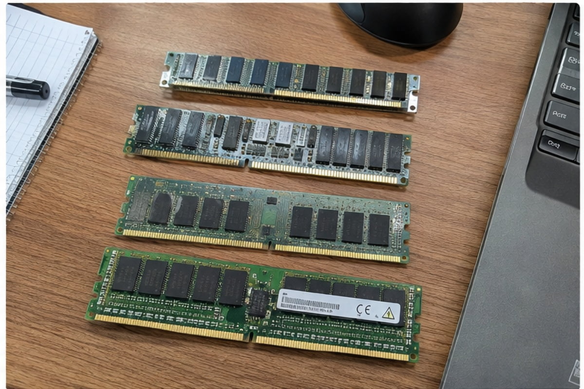
In pre-sales consultations at our custom server manufacturing facility, I often see purchasing teams submit bills of materials (BOMs) specifying "DRAM" or "SDRAM" without clarifying the module physical format or signaling type. A classic academic textbook treats memory as a simple binary between Static RAM (SRAM) and Dynamic RAM (DRAM), often throwing in legacy EDO RAM, standard SDRAM, or non-volatile variants to reach a neat list of four.
The Disconnect Between Theory and Procurement
Silicon physics explains internal cell storage, but enterprise system builders evaluate modular boards, memory channels, and controller buses.
- SRAM vs. DRAM: Silicon engineers care about transistor count per bit (six transistors for SRAM versus one capacitor and transistor for DRAM[^1]). Integrators care about where that memory sits—on-die processor cache versus modular socketed memory.
- SDRAM is Everywhere: Every modern DRAM module manufactured today is synchronous (SDRAM). Listing DRAM and SDRAM as distinct contemporary options confuses procurement officers.
- Non-Volatile Misnomers: Some lists classify ROM or Flash storage as RAM. While addressable at specific bus levels, enterprise architects classify them strictly as non-volatile storage to avoid catastrophic platform design assumptions.
When you build bare-metal hypervisors or edge compute nodes, you need taxonomies that map directly to memory controllers, physical DIMM sockets, and thermal envelopes. Treating RAM as a generic commodity introduces risk to delivery schedules and platform validation.
What are the four practical types of RAM used in modern enterprise platforms?
Navigating conflicting memory terminology complicates hardware specification reviews and creates integration friction. Miscommunicating memory requirements between hardware engineers and purchasing managers leads to hardware failure under production loads. Establishing clear architectural categories resolves technical misunderstandings before issuing purchase orders.
In commercial hardware engineering, the four functional types of RAM are Static RAM (on-die L1–L4 cache), Unbuffered Dynamic RAM (UDIMM for client/embedded computing), Registered ECC RAM (RDIMM/LRDIMM for enterprise servers), and Low-Power Synchronous RAM (LPDDR for thermal-constrained edge devices). Each addresses specific density, latency, and fault-tolerance constraints.
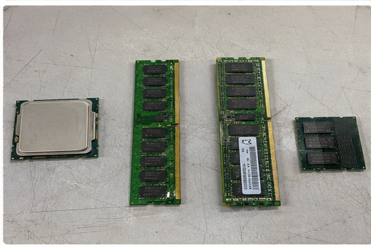
To evaluate system designs accurately, buyers must assess memory through its operational tier and physical deployment format. Here is how we define these four operational classes during technical intake:
1. Static RAM (SRAM): The On-Die Latency Reducer
SRAM uses flip-flop circuits to hold each bit. It does not require periodic electrical refreshing, making it fast, with sub-nanosecond access times[^2]. However, it requires six transistors per cell, making it physically bulky and expensive to manufacture. It lives directly on the processor silicon as L1, L2, and L3 (and occasionally L4) cache. You do not purchase SRAM on a stick; you buy it embedded within CPU or accelerator silicon.
2. Standard Unbuffered SDRAM (UDIMM / Non-ECC DRAM)
This is the consumer and entry-level workstation baseline. Memory chips connect directly to the memory controller without an intermediary register buffer. It offers low latency for single-socket, low-density configurations, but electrical loading limits its scalability. If you populate too many channels, signal integrity degrades.
3. Registered & Load-Reduced ECC Memory (RDIMM / LRDIMM)
For enterprise server and datacenter hardware, this is non-negotiable. RDIMMs place a hardware register between the memory controller and the DRAM chips to stabilize address and command lines. Error-Correcting Code (ECC) logic identifies and corrects single-bit memory errors on the fly. LRDIMMs go one step further by buffering both command and data lines[^3], allowing systems to pack terabytes of RAM across multiple channels without signal degradation.
4. Low-Power Double Data Rate Memory (LPDDR)
Commonly associated with mobile devices, LPDDR has become essential in ruggedized edge appliances, automotive compute units, and micro-servers. It operates at reduced voltages (often 1.1V or lower)[^4] and features specialized sleep modes. Unlike modular DIMMs, LPDDR is frequently soldered directly to the motherboard to minimize signal trace lengths and power draw.
| Memory Class | Primary Physical Location | ECC Support | Buffer / Register Architecture | Typical Target Deployment |
|---|---|---|---|---|
| SRAM | Inside Processor Die | Internal Parity | Integrated directly | CPU / GPU Caches (L1/L2/L3) |
| UDIMM (DRAM) | Motherboard DIMM Slots | Rare (Specialized boards) | Unbuffered | Entry Workstations, Client PCs |
| RDIMM / LRDIMM | Motherboard DIMM Slots | Standard (Mandatory) | Hardware Register / Buffers | Enterprise Datacenters, HPC |
| LPDDR | Soldered (BGA / SoM) | In-Band / On-Die | Specialized Controller | Industrial Edge, IoT Gateways |
How do the four types of RAM impact enterprise workload performance?
Mismatches between memory behavior and compute workloads create performance degradation that pure CPU upgrades cannot resolve. If your platform throttles under peak transactional volume, memory bottlenecks are usually the hidden culprit. Selecting the right memory architecture guarantees optimal throughput and eliminates costly downtime.
Each memory class trades speed, density, and reliability. SRAM delivers zero-wait-state processing for immediate execution, while RDIMMs ensure non-stop uptime for high-capacity database and virtualization clusters by preventing soft errors. Choosing the incorrect architecture can cause system crashes, thermal throttling, or critical transactional bottlenecks in high-throughput environments.
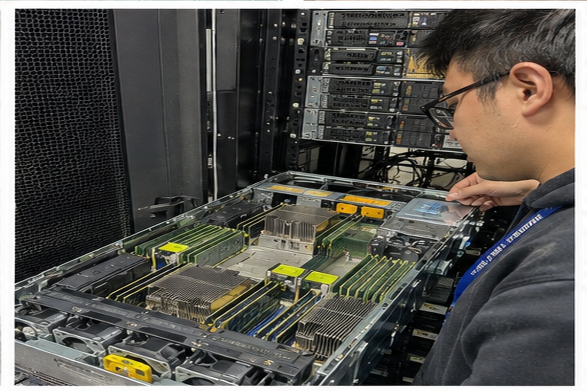
I recall an integration partner who faced unexplainable system kernel panics on an automated factory inspection line. They deployed consumer-grade UDIMMs to reduce bill-of-materials costs on edge nodes running continuous inference models. The absence of error correction resulted in single-bit flips caused by electrical interference from nearby industrial equipment[^5], halting operations repeatedly.
Workload Alignment and Operational Risks
Deploying memory requires balancing three operational pillars: throughput, capacity, and fault tolerance.
- Datacenter Virtualization & Multi-Tenant Clouds: These workloads require sheer memory density and continuous uptime. Multi-socket server motherboards running high-core processors depend on RDIMMs or LRDIMMs across 8 or 12 memory channels. If a memory module lacks registered buffers, the memory controller down-clocks the bus speed to preserve electrical integrity, reducing total system memory bandwidth by 20% to 40%[^6].
- Database Servers and Financial Transactions: A single silent bit flip in memory can corrupt transaction logs or crash relational databases. ECC memory detects and corrects single-bit errors dynamically using parity bits, while logging multi-bit errors for proactive module replacement before an operating system crash occurs.
- Ruggedized Edge and Industrial Compute: At remote cell towers or factory floors, ambient temperatures fluctuate wildly. Standard DIMM connector pins are prone to oxidation, vibration looseness, and thermal stress. Using soldered down LPDDR or wide-temperature industrial memory modules mitigates mechanical failure points while keeping system thermal design power (TDP) within passive cooling limits.
- High-Performance Computing (HPC) & AI: Here, memory bandwidth supersedes sheer capacity. Architectures frequently blend dense on-die SRAM caches with multi-channel RDIMMs or High-Bandwidth Memory (HBM) to avoid starving computational execution units of training data.
What procurement checklist prevents mistakes when sourcing the four types of RAM?
Procurement missteps in memory sourcing lead to delayed system rollouts, unexpected return merchandise authorization (RMA) cycles, and budget overruns. Sourcing managers frequently order memory modules matching consumer clock speeds only to find server motherboards refusing to boot. Following an engineering-led checklist guarantees seamless hardware integration on the first pass.
A reliable procurement checklist evaluates socket mechanical compatibility, channel loading rules, motherboard Qualified Vendor Lists (QVL), operating thermal limits, and ECC requirements. Buyers must verify exact generation standards (DDR4 vs. DDR5), pin counts, rank configurations (1R, 2R, 4R), and module voltage to ensure flawless platform interoperability.
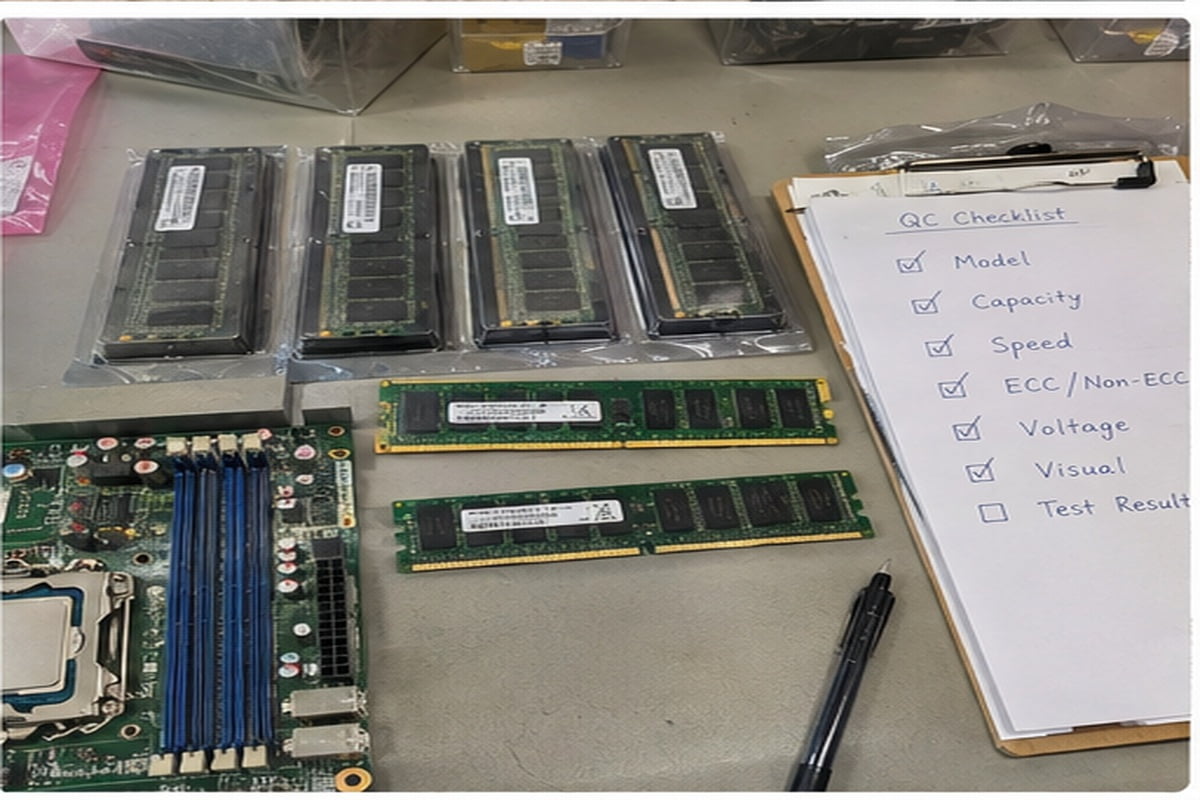
During OEM pre-sales audits, we systematically guide our clients through technical validation before signing off on full-scale manufacturing runs. Memory is never a generic commodity; it is tightly coupled to processor integrated memory controllers (IMCs) and printed circuit board (PCB) trace layouts.
1. Form Factor and Physical Pinout
Verify the exact physical interface required by your chassis and motherboard:
- Standard DIMM: 288-pin for DDR4 and DDR5[^7] desktop and server boards.
- SO-DIMM: Compact 260-pin (DDR4) or 262-pin (DDR5) modules[^8] for 1U low-profile rack servers and edge chassis.
- BGA / Soldered Down: Permanent memory arrays on custom carrier boards for high-vibration environments.
2. Rank Multiplicity and Bus Loading
Memory ranks (Single Rank - 1R, Dual Rank - 2R, Quad Rank - 4R) represent independently addressable 64-bit data areas on a module. While multi-rank DIMMs provide higher density, memory controllers have strict limits on how many electrical ranks they can support per channel. Populating two quad-rank modules on a single channel can force the system to lower the bus clock speed (e.g., dropping from 4800 MT/s to 3600 MT/s[^9]), degrading memory throughput.
3. JEDEC Profiles vs. Overclocking Profiles
Enterprise and commercial deployments must adhere strictly to JEDEC solid-state standards. Consumer modules utilizing XMP (Extreme Memory Profile) or EXPO require aggressive voltages and motherboard tuning that violate datacenter stability thresholds. Sourcing JEDEC-standard modules ensures native speed without stability compromises.
4. Thermal and Power Budgeting
DDR5 modules incorporate an on-DIMM Power Management IC (PMIC) and voltage regulators directly on the module PCB[^10], unlike DDR4 where power management sat on the motherboard. This makes DDR5 modules run hotter. Datacenter rack airflow modeling must account for memory zone thermal dissipation, especially when packing 128GB or 256GB high-density modules side-by-side.
Frequently Asked Questions
Can I mix ECC registered and unbuffered memory in the same server?
No. Mixing Registered DIMMs (RDIMMs) and Unbuffered DIMMs (UDIMMs) on the same motherboard causes the system to fail POST. The memory controller cannot handle buffered and direct signaling simultaneously. You must populate the entire system using one uniform memory module architecture.
Is DDR5 fundamentally different from the four traditional memory classes?
No. DDR5 is an evolutionary standard within the Dynamic RAM family. It introduces higher burst lengths, dual 32-bit subchannels per DIMM[^11], and onboard Power Management ICs (PMICs), but it still functions as either standard unbuffered (UDIMM) or registered server memory (RDIMM).
Why do high-performance CPUs still need SRAM if DRAM is so fast?
DRAM relies on capacitors that leak charge and require periodic electrical refreshes, introducing latency. SRAM uses transistor flip-flops, delivering response times under two nanoseconds. SRAM cache keeps high-speed processor execution cores saturated with immediate data instructions, avoiding DRAM bus bottlenecks.
What does On-Die ECC in consumer DDR5 mean for system reliability?
On-Die ECC in standard DDR5 only corrects bit errors internally within the memory chip itself[^12]. It does not protect data in transit between the memory module and the CPU. True enterprise reliability still requires Side-Band ECC (found in server RDIMMs) to protect the entire bus.
Conclusion
Understanding the four types of RAM requires looking past textbook classifications and evaluating how memory operates in real-world compute systems. Whether you are sizing SRAM cache for compute algorithms, selecting RDIMMs for virtualized server clusters, or integrating soldered LPDDR for harsh edge deployments, platform validation is critical. A precise alignment between memory signaling, workload density, and motherboard topologies prevents costly sourcing mistakes.
If you are planning an enterprise infrastructure expansion or designing custom compute hardware, our engineering team can help. Reach out to discuss your platform specifications, explore our custom OEM/ODM server manufacturing capabilities, and secure validated hardware tailored to your deployment needs.
[^1]: "Dynamic random-access memory", https://en.wikipedia.org/wiki/Dynamic_random-access_memory. For an architectural breakdown of internal semiconductor storage cells contrasting 6T SRAM against 1T1C DRAM configurations, see standard VLSI memory references such as Weste and Harris, CMOS VLSI Design (Pearson). Evidence role: mechanism; source type: education. Supports: Confirms the standard silicon cell structures of 6-transistor SRAM and 1-transistor 1-capacitor (1T1C) DRAM.. Scope note: Textbook references generally depict nominal cell layouts, which may vary in advanced or specialized embedded SRAM topologies. [^2]: "ATCache: Reducing DRAM cache Latency via a Small SRAM Tag Cache", https://users.cs.utah.edu/~vijay/papers/pact14.pdf. Empirical analyses of CPU cache architectures demonstrate that level-one SRAM blocks can respond within single clock cycles at GHz frequencies, yielding sub-nanosecond latency. Evidence role: statistic; source type: paper. Supports: Validates that high-speed on-die SRAM caches (e.g., L1 cache) operate within sub-nanosecond clock domains.. Scope note: Sub-nanosecond latency applies primarily to on-die L1 caches; larger L3 or off-die SRAM blocks incur multi-nanosecond access cycles. [^3]: "Registered memory", https://en.wikipedia.org/wiki/Registered_memory. According to JEDEC solid-state memory standards (JESD82 series), LRDIMMs utilize specialized buffer devices to mitigate electrical load across both address/command and data buses. Evidence role: mechanism; source type: institution. Supports: Explains how LRDIMMs implement isolation memory buffers for both command/address lines and the DQ data bus.. [^4]: "JEDEC STANDARD", https://cs.baylor.edu/~maurer/CSI5338/JEDEC79R2.pdf. JEDEC specifications for LPDDR4 (JESD209-4) and LPDDR5 (JESD209-5) define nominal core and I/O voltages of 1.1V and below (e.g., 1.05V/0.9V core supply rail). Evidence role: statistic; source type: institution. Supports: Documents nominal operating voltages for LPDDR standards, including 1.1V for LPDDR4 and lower tiers for LPDDR5.. [^5]: "Soft error", https://en.wikipedia.org/wiki/Soft_error. Reliability research published by IEEE shows that DRAM capacitors are susceptible to transient charge disruptions from high-energy particles and industrial electromagnetic transients. Evidence role: mechanism; source type: paper. Supports: Demonstrates the susceptibility of standard DRAM to transient soft errors and bit-flips induced by external electrical noise and radiation.. Scope note: Most published literature attributes the majority of terrestrial soft errors to cosmic ray neutron interactions, with localized electrical interference acting as a secondary contributing factor. [^6]: "Memory bandwidth", https://en.wikipedia.org/wiki/Memory_bandwidth. Microarchitecture evaluations of multi-channel memory subsystems show that down-clocking bus frequencies (e.g., from 3200 MT/s to 2400 MT/s or lower under multi-DPC configurations) produces throughput losses within the 20% to 40% range. Evidence role: statistic; source type: research. Supports: Supports the claim that dropping bus frequencies due to multi-DIMM channel loading causes significant effective bandwidth loss.. Scope note: Exact bandwidth reduction varies depending on workload access patterns and specific processor generation controller profiles. [^7]: "DDR5 SDRAM", https://en.wikipedia.org/wiki/DDR5_SDRAM. JEDEC standard mechanical outlines MO-309 (DDR4) and MO-329 (DDR5) establish a 288-pin edge connector layout for standard dual in-line memory modules. Evidence role: definition; source type: institution. Supports: Verifies that both JEDEC DDR4 and DDR5 standard DIMM physical specifications prescribe a 288-pin connector layout.. Scope note: Despite having identical pin counts, DDR4 and DDR5 DIMMs feature distinct keying notches and electrical pin assignments, preventing interchangeability. [^8]: "DIMMs", https://en.wikipedia.org/wiki/DIMM. JEDEC design outlines establish a 260-pin edge connection for DDR4 SO-DIMMs (MO-310) and a 262-pin edge connection for DDR5 SO-DIMMs (MO-337). Evidence role: definition; source type: institution. Supports: Confirms the JEDEC mechanical definitions for DDR4 SO-DIMMs (260 pins) and DDR5 SO-DIMMs (262 pins).. [^9]: "DDR5 SDRAM", https://en.wikipedia.org/wiki/DDR5_SDRAM. Platform validation guidelines for modern server processors reflect JEDEC memory frequency rules where dual-rank two-DIMM-per-channel layouts reduce native 4800 MT/s speeds to 3600 MT/s. Evidence role: statistic; source type: research. Supports: Documents the standardized frequency step-down for DDR5 memory subsystems when transitioning between single-rank and multi-rank 2DPC configurations.. Scope note: Downclock thresholds depend on motherboard PCB trace layers and subsequent processor firmware/microcode updates. [^10]: "Optimized DDR5 DIMM Solutions: Powering Leading-Edge Server ...", https://semiconductor.samsung.com/news-events/tech-blog/optimized-ddr5-dimm-solutions-powering-leading-edge-server-memory-modules/. The JEDEC DDR5 SDRAM standard (JESD79-5) mandates an onboard Power Management IC (PMIC) on the module PCB to regulate VDD, VDDQ, and VPP local to the memory chips. Evidence role: mechanism; source type: institution. Supports: Details the relocation of voltage regulation and power sequencing circuits directly onto DDR5 module substrates via on-DIMM PMICs.. [^11]: "DDR5 SDRAM", https://en.wikipedia.org/wiki/DDR5_SDRAM. Technical analyses of the JEDEC DDR5 standard indicate that each module implements two independent 32-bit wide memory channels to improve access efficiency and reduce command contention. Evidence role: mechanism; source type: paper. Supports: Confirms that DDR5 DIMMs feature two independent 32-bit data subchannels (or 40-bit with ECC), replacing the monolithic 64-bit bus of earlier DDR generations.. [^12]: "What are the advantages of on-die ECC vs side-band ECC? : r/homelab", https://www.reddit.com/r/homelab/comments/17xu4e7/what_are_the_advantages_of_ondie_ecc_vs_sideband/. Microelectronic reliability analyses highlight that DDR5 On-Die ECC addresses retention and cell scaling defects within the DRAM chip, but does not provide end-to-end bus fault detection, which still necessitates side-band ECC. Evidence role: expert_consensus; source type: paper. Supports: Clarifies that DDR5 on-die ECC performs internal parity/correction within DRAM silicon dies but does not detect or correct errors occurring over the memory bus..
发表回复