

Buffered memory is critical for scaling enterprise hard […]
Buffered memory is critical for scaling enterprise hardware platforms, yet selecting the wrong memory architecture can stall an entire server deployment. Misunderstanding module limits leads to unexpected platform lockups, boot failures, and wasted procurement budgets. I frequently guide system integrators through these exact architectural trade-offs to ensure multi-channel compute platforms maintain electrical stability under sustained industrial workloads.
Buffered memory is commonly used in enterprise servers, high-density cloud infrastructure, multi-tenant virtualization platforms, and large-scale database clusters. These mission-critical environments deploy registered DIMMs (RDIMMs) or load-reduced DIMMs (LRDIMMs) across multi-socket systems to stabilize electrical signals, overcome capacitive bus loading[^1], and support massive system memory capacities exceeding several terabytes without compromising platform integrity.
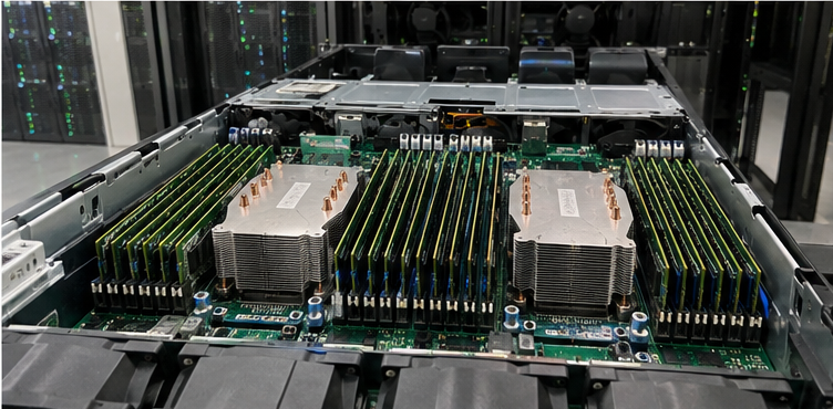
Deciding whether your build requires registered hardware involves far more than reading general marketing sheets. In technical procurement, balancing signal integrity against module latency determines your operational success. Below, I break down the physical constraints, architectural realities, and application profiles that dictate where buffered memory belongs.
Why do enterprise server platforms rely on buffered memory?
High-capacity server builds encounter severe electrical resistance when system integrators populate every available DIMM slot across multi-channel motherboards. Signal degradation creates parity errors, escalating into catastrophic operating system halts and unscheduled downtime. As an OEM hardware consultant, I see engineering teams hit this electrical bottleneck whenever they expand standard multi-channel system memory configurations.
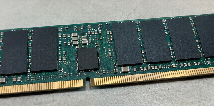
Enterprise server platforms rely on buffered memory to isolate the CPU memory controller from electrical signal loads across dense module configurations. By placing a hardware register directly on the DIMM module, the system reduces capacitive loading on the address and control lines, allowing servers to maintain operational stability across high-slot-count motherboards.
The Physics of Memory Bus Degradation
To understand why enterprise platforms demand registered modules, you must evaluate the physical interface between the integrated memory controller (IMC) and the DRAM chips. In a modern multi-channel server architecture, each CPU channel often links to two or three DIMMs. Every DRAM chip wired directly to that channel adds electrical capacitance to the signal traces.
When you populate multiple unbuffered modules on a single channel, the cumulative capacitance causes signal edge degradation[^2]. The square-wave clock and command signals begin to round off. This distortion creates timing jitter and voltage droop. Consequently, the memory controller can no longer reliably distinguish between a binary zero and a binary one at high clock frequencies.
Direct Bus Loading (Unbuffered / UDIMM):
CPU IMC ───────┬──────────────┬──────────────┬─────── [High Capacitive Load]
               │              │              │
            DRAM 1         DRAM 2         DRAM 3

Isolated Bus Loading (Buffered / RDIMM):
CPU IMC ───────► [ [Register Clock Driver (RCD)](https://ptacts.uspto.gov/ptacts/public-informations/petitions/1558373/download-documents?artifactId=aNsaJtdk3pmW9ioNxVDBBIVNxw6-SCJpH10rjfEtG5NFu9EVHsN3eZ0)[^3] ]      [Low Capacitive Load]
                        │      │      │
                      DRAM 1 DRAM 2 DRAM 3
Mitigating Bus Capacitance with the Register Clock Driver
Buffered memory modules resolve this physics problem by introducing dedicated intermediate hardware:
- The Register Clock Driver (RCD): On a standard Registered DIMM (RDIMM), the RCD sits between the motherboard trace lines and the onboard DRAM chips. The CPU memory controller only communicates directly with this single register chip for command and address instructions.
- Decoupled Electrical Load: The RCD receives the command, regenerates the clean digital signal, and re-drives it locally to the individual DRAM chips on that specific stick. The memory controller sees only a single electrical load per module rather than sixteen or thirty-two distinct loads.
- Scale Without Downclocking: Without buffering, motherboards must drastically drop memory operating frequencies (e.g., throttling down from 4800 MT/s to 3200 MT/s or lower[^4]) as more slots are filled. Buffered memory preserves stable operational frequencies even when populating sixteen to thirty-two DIMM slots per CPU socket.
| Architectural Metric | Unbuffered Memory (UDIMM) | Registered Memory (RDIMM) | Load-Reduced Memory (LRDIMM) |
|---|---|---|---|
| Command/Address Path | Direct to CPU IMC | Buffered by RCD | Buffered by RCD |
| Data (DQ) Line Path | Direct to CPU IMC | Direct to CPU IMC | Buffered by Data Buffers (DB)[^5] |
| Capacitive Bus Load | High (scales per chip) | Low (one command load) | Lowest (fully decoupled) |
| Max Practical Capacity/Node | Modest (<128 GB typical) | High (Up to 4 TB+) | Extreme (8 TB+ on multi-socket) |
| Inherent Latency Overhead | None (Baseline) | +1 Clock Cycle[^6] | +2 to 3 Clock Cycles |
How does buffered memory differ from unbuffered ECC options?
Many procurement managers assume that ordering any component labeled "ECC" provides identical stability across enterprise deployments. This misunderstanding results in rejected production batches, unbootable motherboards, and stalled integration lines. In customer specification reviews, I consistently encounter confusion between data-level error correction algorithms and physical bus buffering.
Buffered memory differs from unbuffered ECC memory because it incorporates a dedicated hardware register to buffer address and command lines, whereas unbuffered ECC (UDIMM) connects directly to the CPU. Both detect and correct single-bit data errors, but only buffered memory mitigates electrical bus loading during high-capacity scaling.
Error Correction vs. Electrical Buffering
Error-Correcting Code (ECC) and memory buffering address two entirely different layers of system engineering. ECC is an algorithmic integrity safeguard implemented at the data layer, while buffering is an analog electrical management technique.
- Unbuffered ECC (ECC UDIMM): These modules carry an extra DRAM chip (yielding a 72-bit bus width instead of 64-bit on DDR4, or dual 40-bit channels on DDR5[^7]). This extra chip stores parity bits. The memory controller executes Hamming code algorithms[^8] to correct single-bit memory errors on the fly. Crucially, the command, address, and clock traces remain directly linked to the CPU without intermediate register chips.
- Registered Memory (RDIMM): RDIMMs almost universally include ECC functionality, but their primary hardware feature is the physical Register Clock Driver. They correct single-bit data errors via ECC while simultaneously shielding the CPU memory bus from the physical capacitance of the memory arrays.
Engineering Rule of Thumb: ECC prevents silent data corruption inside individual bit cells; buffering prevents electrical collapse across the multi-slot memory bus. One guarantees data math; the other guarantees circuit viability.
Why Motherboard Chipsets Prevent Interchanging Them
A frequent pitfall during the bill-of-materials (BOM) creation is attempting to drop registered modules into standard workstation boards. The physical notch on the circuit board might fit the socket, but the machine will not POST (Power-On Self-Test).
CPU manufacturers explicitly divide their silicon tiers based on the Integrated Memory Controller's microcode:
- Consumer and Entry-Level Workstation CPUs: Processors such as entry-level single-socket chips lack the microcode hooks and internal trace timing logic to interface with an RCD chip. They only communicate across raw, direct-attach bus lines. If you insert an RDIMM, the IMC fails to initialize the register, resulting in a black-screen boot failure.
- Enterprise-Class Processors: Server silicon families (such as Intel Xeon Scalable or AMD EPYC) are explicitly engineered to run registered memory topologies. In fact, many of these enterprise processors completely lack support for standard consumer unbuffered memory[^9]. They expect the handoff timing of an RCD module.
Because these memory controller interfaces are mutually exclusive at the hardware level, hardware teams must lock their memory architecture choice before finalizing their motherboard design.
When is buffered memory the wrong architectural choice?
Enterprise buyers often assume top-tier server parts automatically improve performance across every computing scenario. Over-specifying your memory architecture inflates initial bill-of-materials costs while unintentionally introducing latency penalties into performance-critical applications. I always advise system integrators to evaluate their true topological requirements before mandating registered modules across all client hardware platforms.
Buffered memory is the wrong architectural choice for single-socket edge appliances, compact network gateways, lightweight microservers, and low-latency trading workstations. In these setups, module counts are low, meaning bus capacitance remains within safe thresholds, and the inherent one-clock-cycle register latency penalty brings no compensating stability benefits.
The Inherent Latency Penalty
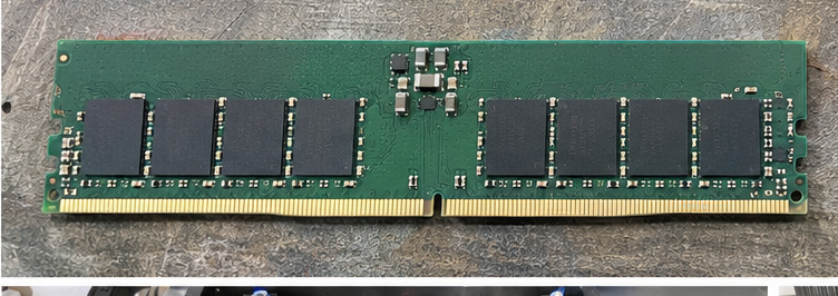
Every hardware register placed in the path of a digital signal introduces a propagation delay. An RDIMM register must latch incoming command and address signals, inspect them, regenerate the waveform, and drive them downstream to the DRAM chips.
- The One-Cycle Tax: This physical re-driving step costs exactly one system memory clock cycle.
- The LRDIMM Tax: If you move to fully buffered Load-Reduced DIMMs (LRDIMMs), where dedicated data buffers also handle the actual data (DQ) bus, you incur additional clock cycle delays on both write and read operations.
In ultra-low-latency computing environments—such as high-frequency trading (HFT) engines or specialized telecom signal-processing pipelines—a 2-to-5 nanosecond memory access penalty degrades trading execution speeds and overall throughput. These applications perform best on high-frequency, unbuffered configurations with low CAS latencies.
The Problem of Diminishing Returns
If a specialized hardware project only requires 32 GB to 64 GB of total system memory, choosing buffered memory delivers zero real-world reliability advantage over unbuffered ECC.
System Density Threshold Analysis:
[ 1 DIMM Per Channel (1 DPC) ] ──► Low Capacitance  ──► Unbuffered ECC is Optimal
[ 2 DIMMs Per Channel (2 DPC) ] ──► High Capacitance ──► Buffered Memory is Mandatory
When you operate just one DIMM per channel (1 DPC) on a modern motherboard:
- The electrical trace length is short.
- The overall bus capacitance remains far below the IMC's maximum electrical tolerance.
- The signal eye diagram remains open and clean without register re-driving.
Under these physical conditions, paying a 15% to 35% premium for registered modules adds bill-of-materials overhead without delivering any measurable uptime improvement.
Thermal and Space Budget Realities
The RCD and data buffer components on a buffered memory module draw active current. On high-density modules, the register chip alone can dissipate 1.5 to 3 watts[^10] of continuous heat.
In compact, fanless 1U network appliances or industrial edge enclosures, this concentrated heat source creates local thermal stress. Without directed airflow across the memory slots, the RCD can hit thermal throttling thresholds. For remote network gateways and edge firewalls, unbuffered ECC provides the required algorithmic data protection while maintaining lower power draw and cooler operational temperatures.
What enterprise applications justify the cost of buffered memory?
System architects must weigh system crash risks against total hardware expenditure during project design phases. Deploying inadequate memory architecture in compute-heavy deployments leads to multi-tenant instability, silent data drops, and costly service level agreement (SLA) breaches. In my custom OEM/ODM hardware work, specific enterprise workloads clearly justify investing in fully buffered architectures.
Enterprise applications justifying the cost of buffered memory include multi-tenant hypervisors, cloud infrastructure nodes, large-scale enterprise resource planning (ERP) databases, and in-memory analytical platforms like SAP HANA[^11]. These applications require multi-terabyte system memory configurations across dozens of slots, making the electrical isolation of registered memory mandatory for uninterrupted operations.
Multi-Tenant Cloud Virtualization
Modern virtualization platforms (such as VMware ESXi, Proxmox VE, and KVM clusters) rely on extreme memory density. Cloud providers sell virtual machines based on CPU core and memory allocations. A dual-socket enterprise server often hosts 64 to 128 virtual machines simultaneously.
- Capacity Over Latency: In a virtualized host, a single-clock-cycle memory delay has no perceptible impact on guest operating system performance.
- Capacity Bottlenecks: The primary constraint is physical density. If a hypervisor runs out of memory, it begins swapping to disk, destroying I/O performance.
- The Slot Populating Mandate: To achieve 1 TB to 4 TB of RAM per node, systems must populate all sixteen or thirty-two motherboard slots. Buffered memory (specifically RDIMMs and LRDIMMs) is the only technology that allows every memory channel to run fully populated at production-grade speeds without bus errors.
Large-Scale In-Memory Databases
In-memory database platforms like SAP HANA, Redis Enterprise, and Apache Ignite hold active data working sets entirely inside physical DRAM. These platforms process millions of analytical transactions per second directly against memory addresses to bypass storage read latency.
Downtime Cost Matrix for High-Density Systems:
[ 4 TB In-Memory Node Crash ] ──► System Reboot: 15-25 Minutes
                              ──► Cold Data Reload from NVMe: 45-90 Minutes
                              ──► Total Business Interruption: > 1 Hour
A crash on an in-memory node due to memory bus degradation triggers an extensive reload cycle. Pulling four terabytes of complex relational data back from NVMe storage arrays into system memory can take over an hour. In these environments, the structural electrical protection offered by registered memory is essential for operational availability.
High-Performance Computing (HPC) and AI Model Pre-Processing
Large-scale computational modeling and AI training pipelines place sustained read-write stress on system memory. While GPU clusters handle the core matrix math, host CPU memory stages massive datasets, formats input tensors, and handles large checkpoint operations.
- Sustained Bus Saturation: Unlike typical office workloads that access memory in sporadic bursts, scientific clustering keeps memory channels continuously saturated for weeks at a time.
- Thermal Drift Protection: Extended multi-week compute runs generate sustained heat that alters copper trace impedance[^12] across server motherboards.
- Signal Margin Preservation: Buffered memory keeps signal margins stable throughout these sustained operational temperature shifts, preventing intermediate computational errors that could ruin lengthy research runs.
Frequently Asked Questions
Can I install buffered memory in a consumer desktop motherboard?
No. Standard consumer desktop motherboards and consumer CPUs lack the firmware microcode and hardware memory controller routing needed to initialize a Register Clock Driver (RCD). Even though the physical slot might match the pin count, the system will fail to complete POST and will not boot.
Does buffered memory always feature ECC protection?
Yes, virtually all modern enterprise buffered memory modules (RDIMMs and LRDIMMs) incorporate ECC error correction logic alongside the physical register. However, unbuffered memory can also feature ECC (UDIMM ECC), so the term "ECC" alone does not indicate whether a module is physically buffered.
What is the operational difference between RDIMM and LRDIMM?
An RDIMM buffers only the command and address bus through a Register Clock Driver, leaving the data (DQ) lines directly wired to the CPU. An LRDIMM (Load-Reduced DIMM) buffers both the command/address lines and the data lines using onboard data buffers, enabling even higher memory slot densities.
Does buffered memory increase system power consumption?
Yes. The Register Clock Driver (RCD) and onboard data buffer logic chips require continuous operational power. Depending on memory clock speeds and module density, a buffered memory module consumes approximately 1.5 to 3 watts more per stick than an equivalent unbuffered consumer DIMM.
Conclusion
Choosing where to deploy buffered memory requires balancing electrical stability against hardware latency and module costs. While registered architectures (RDIMMs and LRDIMMs) add a minor clock-cycle latency penalty and increase component prices, they are necessary for dense, multi-channel server deployments. By isolating capacitive bus loads, buffered memory enables multi-terabyte cloud nodes, enterprise virtualization platforms, and in-memory databases to scale without electrical collapse.
At our OEM/ODM manufacturing facilities, we design and produce enterprise-grade server barebones, high-efficiency power architectures, and tailored compute platforms built for reliable long-term deployment. If you need help validating component specifications, resolving memory bus architectures, or manufacturing custom enterprise hardware at scale, reach out to our engineering team to review your technical requirements.
[^1]: "SecDDR: Enabling Low-Cost Secure Memories by Protecting the DDR ...", https://arxiv.org/html/2209.00685v2. High-speed memory bus analyses demonstrate that parallel capacitive stub loads introduce low-pass filtering effects, narrowing signal eye openings at elevated frequencies. Evidence role: mechanism; source type: research. Supports: Electrical loading and parasitic capacitance scale with the number of attached DRAM components on a shared bus.. Scope note: Specific capacitive tolerances vary based on motherboard trace geometry, layer count, and integrated memory controller PHY specifications. [^2]: "Dynamic random-access memory", https://en.wikipedia.org/wiki/Dynamic_random-access_memory. Transmission line modeling confirms that cumulative lumped capacitance degrades edge rates and induces inter-symbol interference on unbuffered multi-drop memory buses. Evidence role: mechanism; source type: paper. Supports: Added capacitive loading increases signal transition time (slew rate reduction), rounding digital square-wave transitions and creating jitter.. [^3]: "JEDEC STANDARD", https://ptacts.uspto.gov/ptacts/public-informations/petitions/1558373/download-documents?artifactId=aNsaJtdk3pmW9ioNxVDBBIVNxw6-SCJpH10rjfEtG5NFu9EVHsN3eZ0. JEDEC specifications define the Register Clock Driver as an active intermediate device that retimes and redistributes command/address inputs to DRAM devices. Evidence role: definition; source type: institution. Supports: The Register Clock Driver (RCD) buffers control, command, and address lines, presenting a single load per module to the host controller.. [^4]: "DDR5 SDRAM", https://en.wikipedia.org/wiki/DDR5_SDRAM. Platform design guides from major microprocessor vendors mandate frequency step-downs for 2 DIMM per channel (2 DPC) unbuffered configurations to preserve signal margins. Evidence role: statistic; source type: institution. Supports: Integrated memory controllers systematically enforce lower operational transfer rates when multiple unbuffered modules populate a single channel.. Scope note: Exact transition speeds depend on memory generation (e.g., DDR4 vs. DDR5) and motherboard topology (daisy-chain versus T-topology). [^5]: "JEDEC STANDARD", https://ptacts.uspto.gov/ptacts/public-informations/petitions/1558373/download-documents?artifactId=aNsaJtdk3pmW9ioNxVDBBIVNxw6-SCJpH10rjfEtG5NFu9EVHsN3eZ0. Under JEDEC standards, LRDIMMs employ specialized data buffer ICs to convert multiple DRAM electrical loads on the DQ bus into a single virtual load per channel. Evidence role: mechanism; source type: institution. Supports: LRDIMMs isolate both command/address lines and data lines by utilizing distributed data buffer (DB) components on the module.. [^6]: "Registered memory", https://en.wikipedia.org/wiki/Registered_memory. Microarchitectural evaluations confirm that the RCD introduces a deterministic single-cycle pipeline stage to register address and command signals. Evidence role: mechanism; source type: research. Supports: Registering command and address signals through an RCD introduces an inherent one-cycle propagation delay before execution by DRAM banks.. [^7]: "DDR5 SDRAM", https://en.wikipedia.org/wiki/DDR5_SDRAM. The JEDEC DDR5 standard specifies dual 32-bit data channels per DIMM, supplemented by 8 additional ECC bits per subchannel on enterprise modules. Evidence role: definition; source type: institution. Supports: DDR5 architecture splits the conventional 64-bit wide channel into two independent 32-bit channels, expanding to 40 bits each when sideband ECC is implemented.. [^8]: "ECC memory", https://en.wikipedia.org/wiki/ECC_memory. Standard semiconductor memory error correction relies on extended Hamming block codes to detect multi-bit anomalies and autonomously correct single-bit corruptions. Evidence role: mechanism; source type: encyclopedia. Supports: Single-error correction and double-error detection (SECDED) schemes in computer memory typically employ extended Hamming codes.. Scope note: Advanced server architectures may augment classical Hamming codes with Reed-Solomon or chipkill architectures for multi-bit burst correction. [^9]: "CPU for ECC REGISTRED : r/HomeServer", https://www.reddit.com/r/HomeServer/comments/1qar7gw/cpu_for_ecc_registred/. Hardware specifications for enterprise silicon lines (such as Intel Xeon Scalable and AMD EPYC) list support solely for registered and load-reduced modules, omitting UDIMM timings. Evidence role: expert_consensus; source type: research. Supports: Server-grade processors enforce architectural requirements that exclude consumer-grade UDIMMs from supported memory topologies.. Scope note: Some entry-level enterprise processors (e.g., Intel Xeon E series) support unbuffered ECC modules. [^10]: "Micron® DDR5: Key Module Features", https://ptacts.uspto.gov/ptacts/public-informations/petitions/1549629/download-documents?artifactId=oPIV3sHY574B2dSpqs6CcrTGYJKYYXuJcz66kNL94V5NcwQULt6Lbb0. Thermal modeling and component power profiles show enterprise register chips dissipate between 1 and 3 W under sustained high-frequency switching loads. Evidence role: statistic; source type: paper. Supports: Active RCD and data buffer logic components contribute non-trivial static and dynamic power draw to registered modules.. Scope note: Power dissipation varies depending on the operational frequency, supply voltage (e.g., DDR4 1.2V vs. DDR5 1.1V), and bus traffic intensity. [^11]: "Development of a high-performance in-memory database architecture for ...", https://pmc.ncbi.nlm.nih.gov/articles/PMC13180876/. Architectural literature on in-memory databases details the requirement for primary columnar data structures to reside directly in system DRAM during execution. Evidence role: case_reference; source type: paper. Supports: In-memory database engines require entire active transaction sets to reside in physical RAM to maintain near-zero read latencies.. [^12]: "High-Speed PCB Design Guide", https://s3vi.ndc.nasa.gov/ssri-kb/static/resources/High-Speed%20PCB%20Design%20Guide.pdf. Printed circuit board transmission line studies show that thermal variations shift trace resistance and substrate dielectric properties, degrading high-speed signal margins. Evidence role: mechanism; source type: paper. Supports: Elevated operational temperatures increase copper resistivity and alter the dielectric constant of PCB substrates, causing impedance shifts..
发表回复