

Understanding the buffer in RAM is critical when unstab […]
Understanding the buffer in RAM is critical when unstable server deployments threaten project delivery deadlines and hardware budgets. Many system integrators struggle with unexplained memory bus errors and signal degradation under heavy enterprise workloads. Addressing how memory buffers operate across physical hardware and software layers resolves these operational risks before volume deployment begins.
The buffer in RAM refers either to a physical hardware register on an enterprise memory module (such as an RDIMM or LRDIMM) that isolates electrical loads, or to an operating system cache that accelerates storage input/output[^1]. In enterprise computing, both mechanisms prevent data bottlenecks and maintain signal integrity across critical server infrastructure.
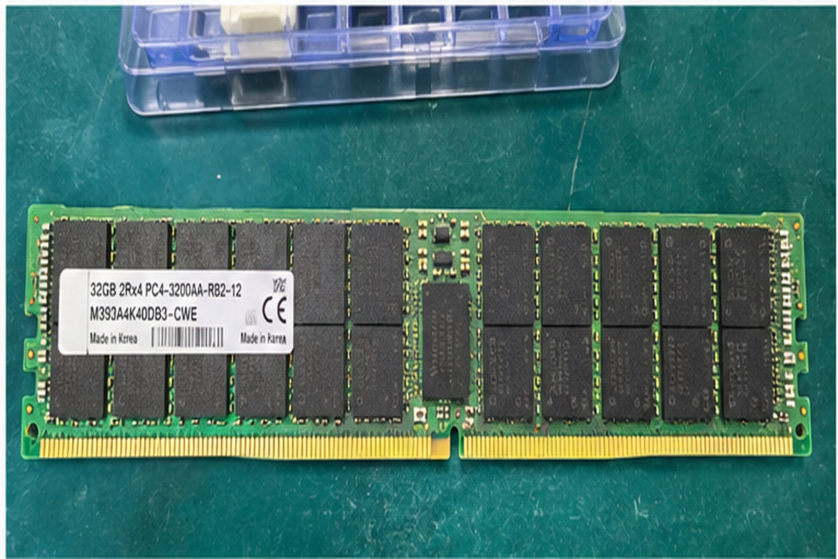
During technical consultations with data center operators, I frequently see these two concepts conflated during bill-of-materials reviews. Distinguishing physical register buffering from operating system disk caching is essential for selecting the correct server architecture. Let us examine how both layers function in production environments.
Why does the buffer in RAM mean two different things?
Procurement teams often misinterpret memory specifications because technical documentation uses identical phrasing for separate hardware and software functions. This semantic overlap causes specification sheets to misalign with actual operational requirements. Clear architectural definitions eliminate costly hardware ordering mistakes and misdiagnosed support tickets.
The term buffer in RAM represents two distinct tiers of enterprise computing: a physical silicon register on server memory modules and an operating system storage cache. Hardware buffers regulate electrical signals across multi-channel motherboards, whereas operating system buffers temporarily hold block device data in system memory to accelerate disk read and write performance.
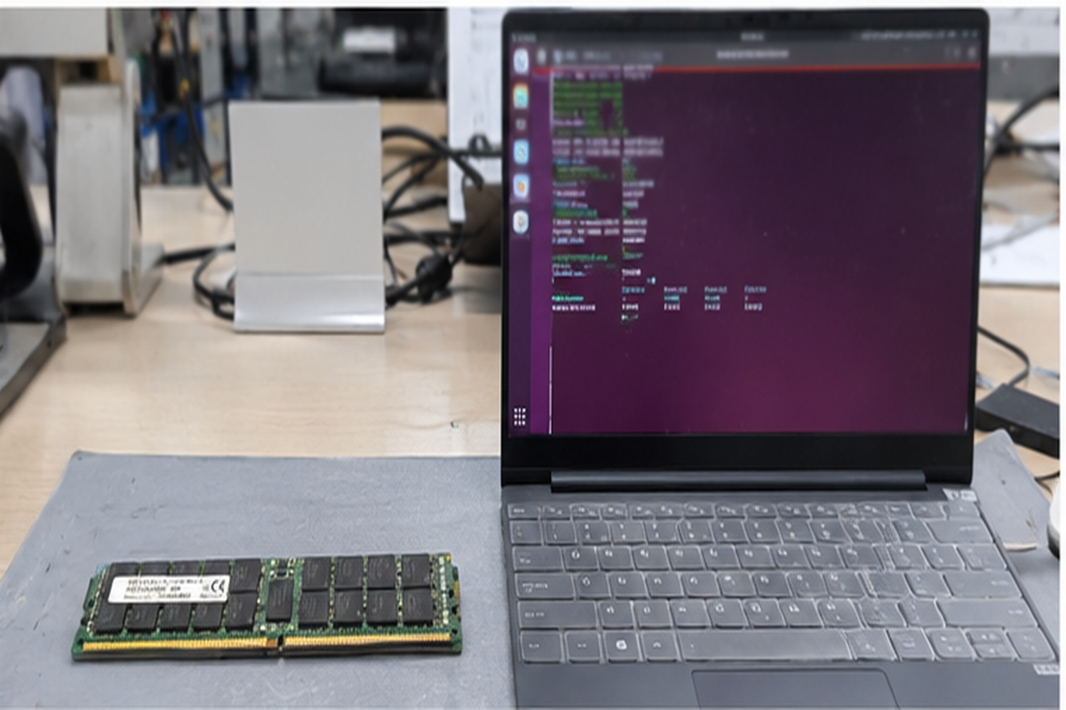
Physical Register Buffers Versus Dynamic Software Caches
To evaluate memory accurately, hardware buyers must decouple the motherboard trace from the software kernel. When a hardware engineer discusses a buffer, they refer to an integrated circuit physically mounted on the Dual In-line Memory Module (DIMM). This chip sits directly between the dynamic random-access memory (DRAM) chips and the host memory controller located on the central processing unit (CPU).
Conversely, when a system administrator or software engineer mentions a memory buffer, they refer to physical memory allocated by the operating system kernel. In Linux environments, for example, the kernel allocates unused RAM to hold filesystem metadata and raw disk blocks[^2]. This dynamic cache speeds up overall system responsiveness by reducing high-latency calls to solid-state drives (SSDs) or mechanical hard drives.
Key Takeaway: Hardware buffers protect electrical stability across physical bus lines. Software buffers optimize data throughput between system storage and active execution memory.
| Architectural Layer | Physical Location | Primary Technical Function | Impact of Misconfiguration |
|---|---|---|---|
| Hardware Buffer | Printed circuit board (PCB) on registered DIMM | Absorbs electrical capacitance and retimes control signals | Unbootable servers, bus parity errors, clock timing violations |
| Software Buffer | Operating system virtual memory allocation | Temporarily holds disk read/write blocks in DRAM | Reduced I/O throughput, misleading memory exhaustion alerts |
Why This Term Conflation Generates Procurement Risk
In my pre-sales conversations, clients sometimes request higher RAM capacity because monitoring tools show zero free memory. They assume their software buffers are overwhelming the server. In reality, the operating system is simply utilizing idle memory productively for disk operations.
Conversely, we see system integrators attempt to cut BOM costs by ordering unbuffered consumer memory modules for dense, multi-socket enterprise servers. When those servers fail during thermal cycling or validation testing, the root cause is not capacity exhaustion. It is the complete absence of a physical hardware buffer on the memory module.
How does a hardware buffer in RAM stabilize enterprise servers?
As data center racks scale up multi-socket architectures, memory channels face extreme electrical capacitance and signal degradation. Without physical isolation, server motherboards experience system halts and parity crashes under heavy multi-threaded loads. Hardware buffering solves this physical signaling dilemma by redistributing electrical loads across the memory bus.
A hardware buffer in RAM stabilizes enterprise servers by placing an intermediate register or data buffer between the memory controller and the dynamic random-access memory (DRAM) chips. This register retimes command, address, and control signals, preventing signal attenuation when populating multiple Dual In-line Memory Modules (DIMMs) per memory channel.
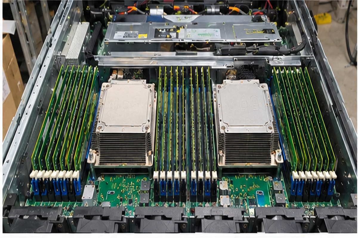
Signal Integrity and Capacitive Loading
Every DRAM chip soldered onto a memory stick adds electrical capacitance to the CPU memory bus[^3]. In consumer desktop systems with only one or two modules per channel, the integrated memory controller handles this electrical load without difficulty. However, enterprise motherboards often feature eight, twelve, or sixteen memory channels, frequently populated with two or three DIMMs per channel (DPC).
When you populate multiple unbuffered DIMMs (UDIMMs) on a single channel, the cumulative capacitive load distorts the high-frequency square wave signals[^4]. The memory controller struggles to distinguish between high and low voltage states, leading to bit flips and system crashes.
A hardware buffer addresses this by acting as an electrical intermediary:
- The CPU memory controller interfaces exclusively with the single buffer chip on the module.
- The buffer chip receives the command and address signals, reconstructs them cleanly, and redistributes them locally to the DRAM chips.
- Electrical load on the CPU memory controller remains constant, regardless of the number of memory chips mounted on the module PCB.
UDIMM, RDIMM, and LRDIMM Structural Trade-offs
Selecting memory requires matching module buffering depth to system channel density. In our OEM manufacturing operations, we categorize enterprise modules into three primary topologies:
[ CPU Memory Controller ]
           |
   +-------+-------+
   |               |
[UDIMM]         [RDIMM]                 [LRDIMM]
(No Buffer)  (Register Buffers       (Data Buffers + Register
Direct Load Command/Address) Buffer All Lines)- Unbuffered DIMMs (UDIMMs): These modules lack registers or buffers. Signals travel directly from the motherboard traces to the DRAM components. They offer the lowest absolute latency but cannot scale past modest capacities or channel densities without electrical instability.
- Registered DIMMs (RDIMMs): These modules incorporate a Registering Clock Driver (RCD). The RCD buffers command, address, and clock signals, while data lines connect directly to the memory controller[^5]. RDIMMs represent the baseline standard for mainstream dual-socket enterprise servers.
- Load-Reduced DIMMs (LRDIMMs): These modules utilize an RCD alongside distributed data buffers (DB). The data buffers isolate both the control signals and the physical data lines (DQ) from the memory controller[^6]. This configuration enables massive memory densities per channel at the expense of slight operational latency.
| Specification Attribute | Unbuffered DIMM (UDIMM) | Registered DIMM (RDIMM) | Load-Reduced DIMM (LRDIMM) |
|---|---|---|---|
| Buffered Signals | None | Command, Address, Clock | Command, Address, Clock, and Data lines |
| Electrical Bus Load | High per chip | Low for control; Standard for data | Lowest overall electrical load |
| Relative Latency | Baseline (Lowest) | +1 Clock Cycle | +2 to 3 Clock Cycles |
| Max System Density | Severely limited | High (Mainstream servers) | Maximum (Hyperscale/HPC) |
| Typical Deployment | Entry edge devices, desktop PCs | Enterprise compute, virtualization | In-memory databases, dense virtualization |
The engineering compromise is straightforward: hardware buffering trades a small latency penalty (typically one clock cycle for an RDIMM[^7]) for massive scalability and electrical reliability.
When does an operating system buffer in RAM indicate real memory pressure?
Infrastructure engineers often worry when monitoring dashboards display ninety percent memory utilization on freshly deployed hypervisors. They assume server capacity is exhausted, leading to premature capital expenditure requests. Understanding operating system memory management clarifies whether memory is genuinely scarce or merely performing standard caching duties.
An operating system buffer in RAM rarely indicates true memory pressure because the kernel automatically reclaims cached disk buffers when active applications request physical memory. True memory pressure only occurs when the system continuously swaps memory pages to secondary storage or when unbuffered application allocations cause Out-Of-Memory (OOM) killer terminations.
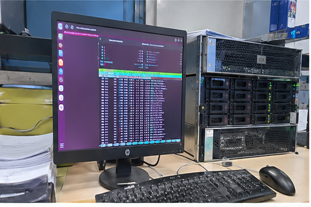
Understanding Buffers and Page Cache in Linux Systems
In modern enterprise operating systems, unused memory is considered wasted resource capacity. Operating system kernels dynamically shift available memory into storage buffers and page caches to reduce storage latency:
- Buffer allocation: The kernel stores raw disk blocks directly in system memory. This holds disk sector writes until they sync to block storage and caches directory structures.
- Page cache allocation: The kernel caches entire file pages mapped from persistent storage systems.
Because read operations from DRAM occur in nanoseconds while NVMe storage operations take microseconds[^8], aggressive caching significantly improves server throughput. Crucially, these buffers are non-retaining allocations. The operating system kernel treats them as immediately discardable. When a database engine or virtual machine requests ten gigabytes of physical memory, the kernel instantly flushes or drops buffered pages and reassigns those physical addresses to the application.
Identifying Genuine Memory Bottlenecks
Procurement teams must train their technical staff to look beyond gross memory utilization metrics before authorizing hardware upgrades. During client diagnostic reviews, we focus on three operational indicators to determine whether a physical capacity upgrade is necessary:
- Available Memory vs. Free Memory: Standard monitoring tools separate "free" memory (unallocated space) from "available" memory. Available memory accurately accounts for reclaimable buffers and caches. If available memory remains healthy, your hardware footprint is sufficient.
- Swap Activity (Si/So Metrics): If an operating system consistently reads and writes memory pages to swap partitions on secondary storage (Swap In/Swap Out), physical memory is exhausted. Swapping introduces massive latency penalties.
- Out-of-Memory (OOM) Invocations: When applications consume all available address space and no reclaimable buffers remain, the kernel invokes its OOM killer to terminate processes[^9]. This indicates genuine hardware deficits.
Evaluating these software behaviors prevents organizations from buying expensive physical modules when their existing hardware balance is operating as intended.
How should procurement teams evaluate the buffer in RAM for custom builds?
Sourcing decisions made solely on unit cost or gross gigabyte metrics risk deploying unstable server hardware in production racks. Substandard memory configurations drive up field failure rates and warranty overhead. A disciplined hardware qualification framework ensures component compatibility, electrical stability, and predictable lifecycle performance.
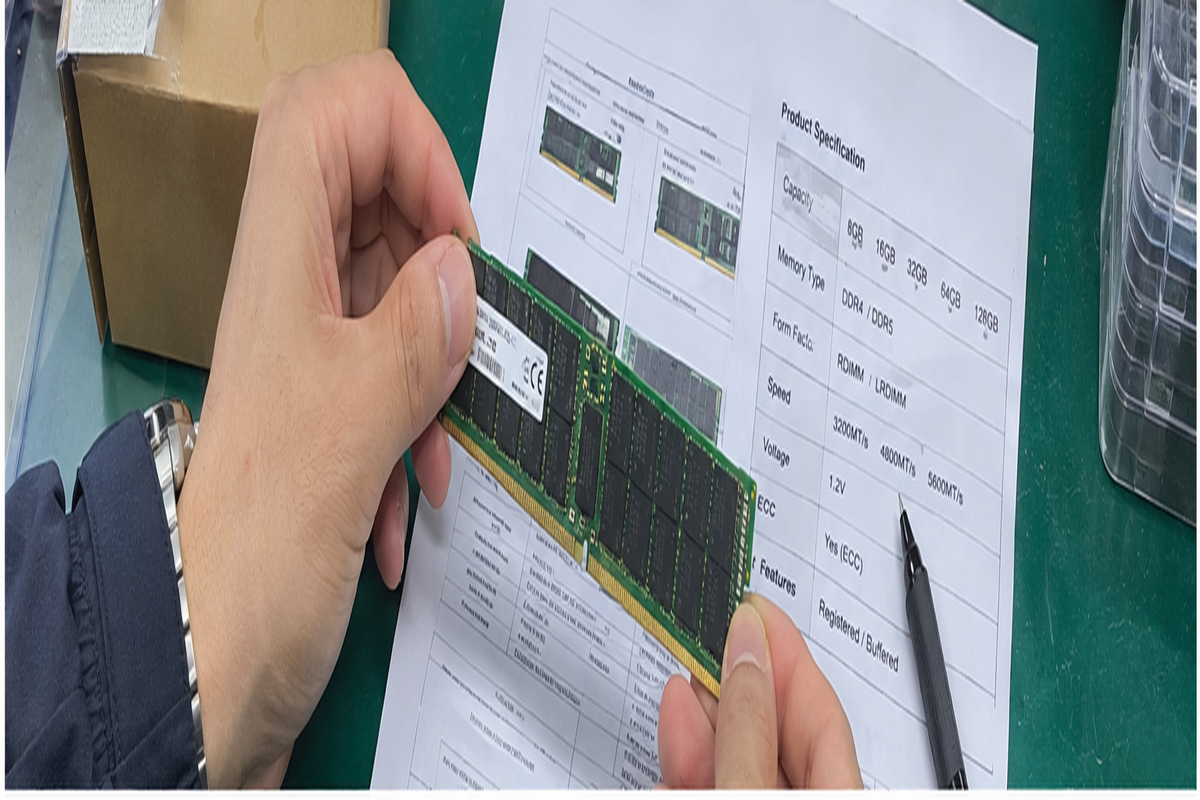
Procurement teams evaluate the buffer in RAM by auditing workload density, target memory channel population, and motherboard chipset qualified vendor lists (QVL). High-density, multi-socket virtualization clusters mandate registered or load-reduced buffering, while dedicated single-socket edge nodes may utilize unbuffered ECC modules to balance acquisition costs and operational latency.
Channel Population Rules and Speed Downgrades
Enterprise memory bus topologies do not run at uniform clock frequencies across all channel configurations. Motherboard manufacturers design trace layouts around strict signaling budgets. When you populate two or three DIMMs per channel to achieve maximum density, the memory controller often forces a lower operating frequency to maintain signal stability[^10].
1 DIMM Per Channel (1 DPC)  --> Native Speed (e.g., DDR5 4800 MT/s)
2 DIMMs Per Channel (2 DPC) --> Frequency Downgrade (e.g., DDR5 4400 MT/s)
3 DIMMs Per Channel (3 DPC) --> Severe Frequency Downgrade / LRDIMM Required
Procurement specialists must balance raw memory capacity against operating frequency requirements:
- Over-specifying unbuffered modules across full channel banks results in non-booting motherboards or spontaneous memory channel dropouts.
- Specifying RDIMMs stabilizes multi-channel layouts with minimal clock latency penalties.
- Utilizing LRDIMMs enables full slot population for memory-intensive workloads, though buyers must verify whether the chassis thermal solution can handle the heat generated by the extra data buffer chips.
Practical Hardware Verification Protocol
Before finalizing an original equipment manufacturer (OEM) build or submitting a volume component order, buyers should execute a four-point verification process:
- Verify Motherboard QVL Documentation: Memory module part numbers must align precisely with the board manufacturer's Qualified Vendor List. A registered buffer from one silicon supplier may behave differently on specific board trace lengths than an alternative supplier's design.
- Cross-Reference JEDEC Profiles: Ensure the module buffer conforms to standardized JEDEC solid-state technical standards[^11] rather than proprietary or consumer-tuned profiles.
- Evaluate Workload Sensitivity to Latency: For high-frequency trading or edge gateway nodes, the added clock cycles of complex buffering could prove counterproductive. For virtualization clusters and cloud platforms, buffering is mandatory to prevent bus errors.
- Establish Strict Bill-of-Materials Controls: Work with your manufacturing partner to lock down component-level revisions. Unannounced substitutions of the Registering Clock Driver (RCD) revision can break platform certifications mid-lifecycle.
By treating physical memory buffering as an architectural requirement rather than a generic commodity spec, procurement teams safeguard system uptime and optimize operational spend.
Frequently Asked Questions
Does a hardware buffer in RAM increase memory latency?
Yes, a hardware buffer in RAM introduces a slight latency increase. The register on an RDIMM delays command and address signals by one clock cycle to verify and retime electrical signaling. Load-reduced memory modules add minor additional latency to isolate data lines. However, this small latency trade-off allows servers to support significantly higher densities and remain electrically stable.
Can you mix buffered and unbuffered RAM on the same server motherboard?
No, you cannot mix buffered and unbuffered RAM within the same system[^12]. Motherboard memory controllers configure their physical signaling parameters for either direct-attached or registered module topologies. Installing unbuffered DIMMs alongside registered or load-reduced DIMMs disrupts signaling, triggers BIOS memory initialization errors, and prevents the system from booting successfully.
Why does Linux show low free memory when the buffer in RAM is full?
Linux handles memory efficiently by allocating unused physical space to disk buffers and page caches. This strategy accelerates system input/output performance. The kernel considers this memory fully reclaimable. If an application demands physical memory, the operating system instantly releases buffered storage blocks to satisfy the application's requirements without performance degradation.
What is the primary operational difference between RDIMM and LRDIMM buffers?
An RDIMM buffers only the command, address, and clock control lines using an onboard Registering Clock Driver, leaving data lines connected directly to the CPU. An LRDIMM buffers both control signals and data lines using distributed data buffers. This extra layer lowers electrical bus load, allowing higher module density per channel.
Conclusion
Understanding the buffer in RAM requires distinguishing between physical circuit isolation and operating system memory caching. In enterprise computing, hardware buffering maintains vital electrical signal integrity across dense multi-channel platforms, while operating system software buffering accelerates storage throughput. Confusing these two functions leads to poor hardware purchasing decisions, unnecessary capital expenditures, and platform instability.
As an OEM/ODM hardware manufacturer, we specialize in helping system integrators and enterprise operators configure validated, production-ready server platforms. If you are designing next-generation computing infrastructure or need reliable hardware lifecycle management, contact our engineering team today to review your technical specifications.
[^1]: "Registered memory", https://en.wikipedia.org/wiki/Registered_memory. Documented in architectural overviews of enterprise computer systems and operating systems, which define hardware registers on memory modules separately from kernel-managed I/O buffers. Evidence role: definition; source type: encyclopedia. Supports: The dual technological usage of 'buffer' in both memory hardware registers and operating system page/buffer caches.. [^2]: "Kernel Buffer Cache", https://pdos.csail.mit.edu/archive/exo/exo-internals/node11.html. Described in operating systems literature (such as Bovet and Cesati's analysis of the Linux kernel architecture), showing how page caches and buffer heads manage block I/O. Evidence role: mechanism; source type: education. Supports: The Linux kernel's use of spare physical memory to cache disk blocks and filesystem structures.. [^3]: "Dynamic random-access memory", https://en.wikipedia.org/wiki/Dynamic_random-access_memory. Validated by electrical engineering studies on high-speed DRAM bus topologies, where parallel package stubs introduce cumulative trace capacitance. Evidence role: mechanism; source type: paper. Supports: That placing additional DRAM packages on a bus trace introduces capacitive load, attenuating high-frequency signal integrity.. [^4]: "Multi-Drop Bus / Internal Communication Protocol", https://en.wikipedia.org/wiki/Multi-Drop_Bus_/_Internal_Communication_Protocol. Demonstrated by signal integrity evaluations of multi-drop DDR topologies showing reduced timing and voltage margins under heavy capacitive loads. Evidence role: mechanism; source type: research. Supports: Excess capacitive loading in multi-drop unbuffered memory buses leads to severe eye-diagram degradation and signaling errors.. Scope note: Signal distortion varies significantly depending on bus frequency, trace geometry, and termination impedance. [^5]: "Memory Structure", https://www.cs.emory.edu/~cheung/Courses/355/Syllabus/3-memory/memory.html. Defined by JEDEC Solid State Technology Association standards for DDR registered memory module pinouts and RCD operational specifications. Evidence role: definition; source type: institution. Supports: RDIMM architecture isolates control, command, and clock signals via an RCD while routing DQ data lines directly to the controller.. [^6]: "Performance and Energy Benefits of MRDIMMs", https://arxiv.org/html/2605.02371v1. Specified in JEDEC memory design standards for load-reduced dual in-line memory modules, establishing data buffer placement to decouple electrical loads. Evidence role: mechanism; source type: institution. Supports: LRDIMMs isolate both command/address lines and physical data lines (DQ) using a central RCD and peripheral data buffers.. [^7]: "Memory timings", https://en.wikipedia.org/wiki/Memory_timings. Confirmed by DRAM architectural benchmark papers and JEDEC specifications documenting the t_CDM / registered delay penalty. Evidence role: statistic; source type: paper. Supports: An RDIMM's RCD incurs an intrinsic one-cycle register delay during command and address propagation.. Scope note: Applies strictly to command and address phases; read and write data path latencies are governed by standard CAS timings. [^8]: "Memory hierarchy – Clayton Cafiero", https://www.uvm.edu/~cbcafier/cs2210/content/07_memory_hierarchy/memory_hierarchy.html. Established in computer architecture literature (e.g., Hennessy and Patterson) comparing primary DRAM access times (~50-100 ns) with flash/NVMe access times (~10-100 μs). Evidence role: statistic; source type: research. Supports: The orders-of-magnitude performance gap between nanosecond DRAM access and microsecond NVMe solid-state storage access.. [^9]: "[PATCH 4.14 195/251] mm, oom: do not trigger out_of_memory from the ...", https://lkml.iu.edu/2111.3/00840.html. Documented in Linux kernel documentation on memory management and the out-of-memory killer subsystem (mm/oom_kill.c). Evidence role: mechanism; source type: other. Supports: The mechanism whereby the Linux kernel triggers the OOM killer upon total allocation failure when reclaimable pages are depleted.. [^10]: "Does 2 DIMM per Channel RAM Impact Content Creation Performance?", https://www.pugetsystems.com/labs/articles/does-2-dimm-per-channel-ram-impact-content-creation-performance/. Detailed in enterprise server processor guidelines (such as Intel and AMD platform memory configuration guides), which map supported MT/s rates against 1 DPC and 2 DPC populations. Evidence role: mechanism; source type: research. Supports: Multi-DIMM per channel configurations necessitate operating frequency downgrades due to bus electrical topology constraints.. [^11]: "JEDEC memory standards", https://en.wikipedia.org/wiki/JEDEC_memory_standards. Referenced in JEDEC Solid State Technology Association publications governing DDR memory module, RCD, and Data Buffer device standards. Evidence role: definition; source type: institution. Supports: JEDEC is the primary international engineering authority standardizing memory module architectures, pinouts, and register chips.. [^12]: "Registered memory", https://en.wikipedia.org/wiki/Registered_memory. Consistently documented in motherboard architectural guidelines and memory subsystem documentation, which specify that PHY timing registers cannot drive mixed topologies. Evidence role: expert_consensus; source type: education. Supports: Memory controllers enforce mutually exclusive configuration modes for registered versus unbuffered signalling..
发表回复