

Identifying the two different types of RAM sounds like […]
Identifying the two different types of RAM sounds like a straightforward technical inquiry, but commercial confusion often derails enterprise hardware budgets. Sourcing the wrong memory class leads to platform boot failures, uncorrectable data corruption, and expensive supply chain delays. Clarifying these operational distinctions protects your hardware deployment from costly architectural mismatches before issuing a purchase order.
The two different types of RAM at an engineering level are Static RAM (SRAM) and Dynamic RAM (DRAM). In commercial enterprise procurement, however, buyers practically evaluate two different types of RAM based on operational architecture: Error-Correcting Code (ECC) versus Non-ECC memory, alongside generational deployment standards like DDR4 versus DDR5.
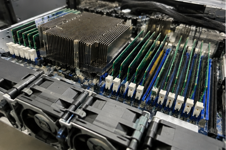
Textbooks explain the silicon physics of memory, but enterprise hardware buyers cannot purchase individual SRAM sticks for a server build. We must look beyond classroom theory and focus on how physical memory selection drives stability, platform compatibility, and total ownership costs across production environments.
Are SRAM and DRAM the two different types of RAM you actually buy?
Procurement teams often waste valuable time reviewing semiconductor definitions that provide zero practical value during server configuration. Sourcing non-existent modular parts delays projects and frustrates engineering stakeholders. Distinguishing component-level silicon from modular platform memory eliminates this confusion immediately.
The two different types of RAM in physical computing are Static RAM (SRAM) and Dynamic RAM (DRAM). However, enterprise buyers only procure DRAM in the form of DIMM modules. SRAM cannot be bought separately because manufacturers integrate it directly onto the processor die as ultra-fast L1, L2, and L3 cache memory.
The Practical Silicon Divide
In my technical pre-sales consultations, clients occasionally ask if they can order high-capacity SRAM cards to accelerate specific machine learning workloads. I explain that computer architecture does not work that way.
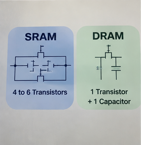
SRAM uses a multi-transistor design (typically four to six transistors per bit cell[^1]) without needing capacitive refresh cycles. This design makes SRAM blazingly fast, but it consumes vast silicon real estate and generates high thermal output. CPU designers reserve SRAM strictly for on-chip cache.
DRAM, on the other hand, uses a compact design comprising a single transistor and a single capacitor per bit cell[^2]. Because capacitors leak charge, DRAM requires periodic electronic refresh cycles every few milliseconds to retain data. This refresh process introduces slight latency, but it enables the massive memory density required for modern enterprise workloads.
| Architecture Characteristic | Static RAM (SRAM) | Dynamic RAM (DRAM) |
|---|---|---|
| Basic Cell Structure | 4 to 6 transistors | 1 transistor + 1 capacitor |
| Data Retention | Continuous while powered | Requires periodic refresh cycles |
| Speed / Access Time | Sub-nanosecond latency[^3] | 10 to 60 nanoseconds latency |
| Silicon Density | Low density, high footprint | High density, small footprint |
| Procurement Form Factor | Soldered on-die (L1/L2/L3 CPU cache) | Swappable modules (DIMMs / SO-DIMMs) |
| Purchasable as a Spare? | No (integrated with CPU) | Yes (standard procurement item) |
When you issue a Request for Quotation (RFQ) for system memory, you are exclusively purchasing DRAM. Within this domain, the actual hardware selection branches into functional reliability classes and generational interfaces.
Why are ECC and Non-ECC the two different types of RAM enterprise buyers evaluate?
Deploying unverified memory into mission-critical infrastructure risks silent data corruption, kernel panics, and catastrophic service interruptions. Hardware buyers face severe reputational and financial fallout when memory faults crash production databases. Choosing the correct operational memory type prevents costly enterprise downtime.
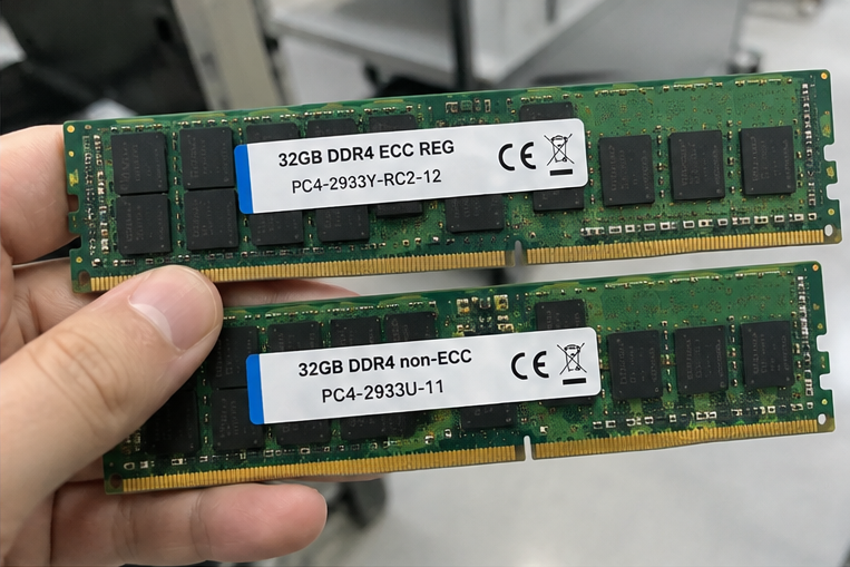
When evaluating system reliability, ECC (Error-Correcting Code) and Non-ECC represent the two different types of RAM that drive commercial decisions. ECC memory contains additional physical memory chips that detect and correct single-bit memory errors in real time, whereas Non-ECC RAM allows undetected memory flips to crash systems or corrupt files.
Mitigating Electrical Noise and Soft Errors
Cosmic radiation, magnetic interference, and electrical background noise constantly threaten server stability.[^4] These environmental factors cause spontaneous state changes in memory cells, known as single-bit flips.
Standard consumer computers use Non-ECC memory. When a bit flips in a desktop running a consumer operating system, an application might crash, or a blue screen occurs. In an enterprise storage cluster, a single-bit flip can permanently corrupt a customer database or disrupt financial ledger calculations.
ECC modules add an extra 8 bits of parity data for every 64 bits of bandwidth.[^5] The memory controller runs an algorithmic parity check (usually Hamming code) to dynamically catch and repair single-bit errors without interrupting the operating system. If a catastrophic multi-bit error occurs, ECC memory halts the system gracefully to prevent corrupt data from writing to enterprise storage arrays.
Sub-Categories: UDIMM, RDIMM, and LRDIMM
Procuring ECC memory requires navigating further hardware sub-classes:
- ECC UDIMM (Unbuffered DIMM): Offers basic ECC error correction with unbuffered lines. These modules connect directly to the memory controller. They suit entry-level branch office servers and micro-appliances, but they limit memory capacity per channel.
- RDIMM (Registered DIMM): Features a dedicated register chip between the DRAM modules and the CPU memory controller[^6]. The register buffers control and address signals, reducing electrical load. This allows system builders to install significantly higher memory capacities across multiple channels without signal degradation.
- LRDIMM (Load-Reduced DIMM): Buffers both memory addressing and data lines using a specialized memory buffer.[^7] LRDIMMs maximize rank capacity in dense multi-socket virtualization hosts, though they introduce minor latency trade-offs.
Motherboards and CPUs dictate support for these modules. An enterprise platform engineered for Registered ECC (RDIMM) will fail to boot if fitted with unbuffered consumer Non-ECC DIMMs.
How do DDR4 and DDR5 represent two different types of RAM for platform migrations?
Assuming modern memory standards can seamlessly mix into existing compute platforms triggers severe procurement waste and project delays. Forcing incompatible memory standards halts production schedules and ruins component budgets. Knowing when to upgrade or maintain generational standards ensures stable lifecycle management.
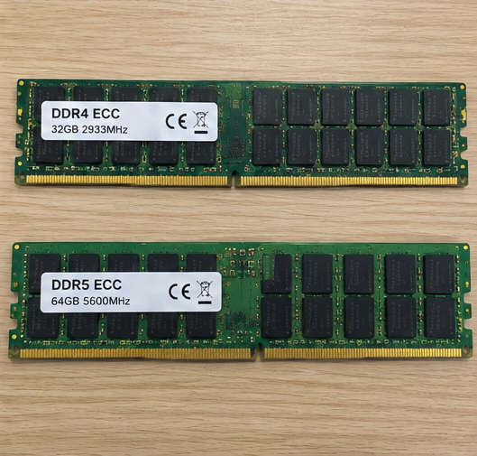
DDR4 and DDR5 represent the two different types of RAM dominating modern platform migrations and procurement lifecycles. DDR5 doubles data transfer rates and moves voltage regulation onto the physical memory stick, but it features an entirely incompatible pinout and key notch layout compared to legacy DDR4 infrastructure.
The Incompatibility Pitfall
In my experience advising system integrators, a frequent procurement error occurs when buyers treat DDR5 as a drop-in replacement for aging DDR4 compute nodes. DDR4 and DDR5 modules are physically and electrically incompatible. DDR4 modules use a 288-pin interface with a specific mechanical alignment notch[^8], while DDR5 uses a differently positioned 288-pin layout to prevent mechanical insertion into older sockets.
DDR4 Module Layout:
[=======================  |  =======================]
(Key Notch: Offset towards center-left)

DDR5 Module Layout:
[=====================  |  =========================]
(Key Notch: Repositioned; Onboard PMIC integrated)
Beyond physical mechanics, the power architecture changed completely between generations:
- DDR4 Power Architecture: The server motherboard manages power distribution. A dedicated voltage regulator down-converts input power to 1.2V across the memory bus.
- DDR5 Power Architecture: The memory module manages its own power. Each DDR5 DIMM features an integrated Power Management IC (PMIC) running at 1.1V.[^9] This improves voltage regulation and reduces motherboard circuit complexity, but it increases the unit cost of individual DDR5 modules.
Architectural Performance Metrics
DDR5 introduces independent 32-bit subchannels (plus an extra 8 bits of subchannel ECC on enterprise sticks) per DIMM.[^10] This dual-subchannel architecture significantly enhances access efficiency compared to DDR4’s single 64-bit bus.
| Technical Parameter | DDR4 Memory Standard | DDR5 Memory Standard |
|---|---|---|
| Standard Data Rates | 2133 to 3200 MT/s | 4800 to 6400+ MT/s |
| Standard Operating Voltage | 1.2V | 1.1V |
| Power Management Location | Motherboard circuitry | On-DIMM PMIC |
| Channel Architecture | 1x 64-bit channel per stick | 2x 32-bit subchannels per stick |
| On-Die Error Correction | Optional / Platform Dependent | Standard on all bare silicon[^11] |
| Cost Profile per Gigabyte | Mature, low cost | Premium enterprise pricing |
DDR5 delivers clear performance advantages for memory-bound virtualization, high-density computing, and AI inference engines. However, DDR4 remains the rational, cost-effective choice for industrial compute appliances, edge firewalls, and cold-storage management servers where platform maturity and supply chain stability outweigh sheer bandwidth.
Which checklist validates these two different types of RAM before issuing a purchase order?
Issuing a large purchase order without checking hardware compatibility leads to expensive inventory write-downs and protracted vendor disputes. Procurement teams cannot rely on generic memory spec sheets alone. Executing a standardized technical checklist guarantees flawless integration across your target hardware fleet.
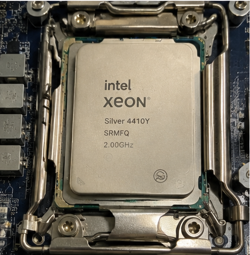
Validating these two different types of RAM requires cross-referencing your target processor's integrated memory controller (IMC) capabilities, verifying physical space limits, and consulting the motherboard manufacturer's Qualified Vendor List (QVL). This structured engineering process verifies memory compatibility prior to component delivery.
The Pre-Procurement Engineering Review
Before authorizing capital allocation for system memory, I guide hardware procurement managers through four validation stages:
1. Check Processor IMC and Chipset Constraints
Every system processor carries firm physical limits regarding maximum memory capacity, supported transfer speeds, and channel counts.
- Check the vendor documentation (such as Intel ARK or AMD Processor Specifications) for the exact processor SKU.
- Confirm whether the processor supports your chosen memory class (for instance, certain edge processors support ECC UDIMM but refuse RDIMM).
- Verify memory speed de-rating rules. Many enterprise CPUs reduce overall memory frequency when you populate two DIMMs per channel (2DPC) versus one DIMM per channel (1DPC).[^12]
2. Verify the Motherboard QVL (Qualified Vendor List)
Server board manufacturers publish extensive QVL documentation detailing every memory module certified for stable operation.
- Match the exact manufacturer part number (MPN), including internal timing suffixes, against the board builder's QVL.
- If a module does not appear on the official QVL, ask your OEM partner to run an electrical validation test on sample modules before committing to production volumes.
3. Account for Physical Enclosure Clearances
Server chassis often impose severe thermal and dimensional constraints on memory modules.
- Standard 1U rackmount chassis paired with passive heat sinks may require Very Low Profile (VLP) memory modules to maintain uninhibited airflow across the chassis.
- Ensure thermal spreaders installed on third-party memory modules do not foul CPU heatsinks, air shrouds, or storage backplane cabling.
4. Review Channel Balancing and Population Topology
Modern server architectures require precise memory population schemes to deliver advertised memory bandwidth.
- Review the platform installation manual to determine symmetrical channel population rules (such as matching sets of 4, 8, or 12 channels per CPU socket).
- Avoid mixing memory densities, ranks, or operational speeds across the same memory bank. Mixing modules causes the memory controller to downclock to the slowest installed stick, wasting expensive system performance.
Frequently Asked Questions
What are the two main types of RAM found in personal computers?
In consumer personal computers, the two primary operational types of RAM are DDR4 and DDR5 Dynamic RAM. These memory modules use Non-ECC unbuffered architecture (UDIMM) designed for basic computing tasks, web browsing, and consumer gaming workloads where hardware-level error correction is not required.
Can you install ECC RAM on a standard consumer desktop motherboard?
Most consumer motherboards will not boot with registered ECC (RDIMM) memory modules because consumer CPUs lack the necessary register clock support. Some consumer AMD processors accept unbuffered ECC (ECC UDIMM) modules, but they typically operate without active error-correcting features unless the motherboard BIOS explicitly supports it.
What is the main difference between SRAM and DRAM?
SRAM retains data using a multi-transistor flip-flop circuit and does not need to be refreshed, making it fast and expensive. DRAM stores data in a capacitor-transistor cell that leaks charge and requires continuous electrical refresh cycles, making it slower but far denser and cheaper to manufacture.
Can DDR4 and DDR5 memory modules be mixed on the same server motherboard?
No. DDR4 and DDR5 memory modules use entirely different electrical pin architectures, signal paths, operating voltages, and physical alignment notches. A motherboard memory slot accepts either DDR4 or DDR5, but it can never physically or electrically support both generations simultaneously.
Conclusion
Determining the two different types of RAM involves more than basic semiconductor definitions. While SRAM and DRAM represent the theoretical divide, hardware buyers face operational decisions balancing ECC reliability against Non-ECC costs, or coordinating generational platform upgrades between DDR4 and DDR5. Overlooking these practical requirements leads to platform instability, motherboard incompatibilities, and unexpected capital losses.
As an OEM/ODM hardware partner, we design, manufacture, and integrate enterprise computing platforms, server chassis, and power subsystems built to your precise hardware specifications. Contact our engineering pre-sales team today to review your hardware requirements, validate memory topologies, and streamline your production delivery pipeline.
[^1]: "Static random-access memory", https://en.wikipedia.org/wiki/Static_random-access_memory. Describes conventional CMOS SRAM bit-cell architectures, highlighting the standard six-transistor (6T) cross-coupled latch configuration. Evidence role: mechanism; source type: encyclopedia. Supports: Standard static RAM bit cells are implemented using four to six transistors forming cross-coupled inverters.. [^2]: "Dynamic random-access memory", https://en.wikipedia.org/wiki/Dynamic_random-access_memory. Outlines the fundamental 1T1C storage element of dynamic random-access memory and the technical necessity of refresh operations. Evidence role: definition; source type: education. Supports: DRAM cells store individual bits using a single transistor and single storage capacitor (1T1C) subject to charge decay.. [^3]: "Memory Hierarchy in 10 Minutes - CSSE 132", https://www.rose-hulman.edu/class/csse/csse132/2627a/memory-hierarchy-review.html. Surveys the memory hierarchy, documenting order-of-magnitude latency differences between on-die cache and modular dynamic main memory. Evidence role: statistic; source type: education. Supports: On-chip SRAM cache access times operate below one nanosecond, whereas off-chip DRAM typically requires tens of nanoseconds.. Scope note: Real-world latencies depend heavily on CPU clock frequencies, bus topologies, and memory controller overhead. [^4]: "Soft error", https://en.wikipedia.org/wiki/Soft_error. Details how high-energy atmospheric neutrons induce charge displacement in silicon, generating soft errors in DRAM arrays. Evidence role: mechanism; source type: paper. Supports: Atmospheric neutrons originating from cosmic radiation cause single-event upsets (bit flips) in terrestrial semiconductor memory.. [^5]: "ECC memory", https://en.wikipedia.org/wiki/ECC_memory. Explains the implementation of Hamming-derived SECDED parity codes over 72-bit memory buses in fault-tolerant computer architectures. Evidence role: mechanism; source type: encyclopedia. Supports: ECC DIMMs utilize a 72-bit interface (64 data bits plus 8 check bits) to facilitate single-error correction and double-error detection (SECDED).. [^6]: "Registered memory", https://en.wikipedia.org/wiki/Registered_memory. Documents JEDEC design rules for registered memory modules, specifying how the RCD stabilizes signal integrity across dense multi-rank configurations. Evidence role: mechanism; source type: institution. Supports: RDIMMs buffer command, address, and clock signals through an onboard register to minimize capacitive loading on host memory channels.. [^7]: "UDIMM, RDIMM, and LRDIMM | Exxact Blog", https://www.exxactcorp.com/blog/HPC/differences-between-dual-in-line-memory-modules-rdimm-vs-lrdimm. Defines JEDEC specifications for LRDIMM architectures, illustrating how bidirectional data buffers reduce bus electrical loading. Evidence role: definition; source type: institution. Supports: Load-Reduced DIMMs replace the traditional register with memory buffers that isolate both control/address signals and data lines from the host bus.. [^8]: "DDR4 SDRAM", https://en.wikipedia.org/wiki/DDR4_SDRAM. Defines the electrical pin assignments and mechanical outline for DDR4 SDRAM unbuffered and registered modules under JEDEC standard JESD79-4. Evidence role: definition; source type: institution. Supports: Standard DDR4 DIMM modules feature a 288-pin connector layout with a specified off-center mechanical alignment notch.. [^9]: "DDR5 SDRAM", https://en.wikipedia.org/wiki/DDR5_SDRAM. Specifies DDR5 module power distribution under JEDEC JESD79-5, outlining PMIC voltage step-down and localized telemetry capabilities. Evidence role: mechanism; source type: institution. Supports: DDR5 architecture lowers core operating voltage to 1.1V and integrates a dedicated Power Management IC directly onto the module substrate.. [^10]: "DDR5 SDRAM", https://en.wikipedia.org/wiki/DDR5_SDRAM. Analyzes the DDR5 dual-subchannel memory interface, illustrating how dual independent subchannels mitigate command/data bus contention. Evidence role: mechanism; source type: research. Supports: Each DDR5 module implements two independent 32-bit data channels (expanding to 40-bit for side-band ECC) to enhance burst efficiency.. [^11]: "DDR5 ECC Explained: On-Die ECC vs Side-Band ECC", https://www.atpinc.com/tw/blog/ddr5-what-is-on-die-ecc-how-is-it-different-to-traditional-ecc. Clarifies JEDEC requirements for internal on-die ECC in DDR5 devices, distinguishing internal bit correction from full system-level bus ECC. Evidence role: definition; source type: institution. Supports: DDR5 specifications require on-die ECC within the memory chip to manage internal cell reliability at high scaling densities.. [^12]: "Am I interpreting this 1DPC vs 2DPC table correctly : r/buildapc", https://www.reddit.com/r/buildapc/comments/164de1v/am_i_interpreting_this_1dpc_vs_2dpc_table/. Examines electrical bus loading in high-density multi-channel server platforms, documenting frequency step-downs between 1DPC and 2DPC layouts. Evidence role: general_support; source type: research. Supports: Signal integrity degradation from capacitive loading in two-DIMM-per-channel topologies frequently necessitates clock frequency de-rating.. Scope note: Exact de-rating thresholds vary across processor generations and specific motherboard trace routing implementations.
发表回复