

Procurement teams often ask if server RAM can swap dire […]
Procurement teams often ask if server RAM can swap directly into standard desktop motherboards to cut build costs. Mixing these component classes creates immediate boot failures, unstable firmware states, and expensive deployment delays across your enterprise infrastructure. You can avoid wasted capital and hardware damage by understanding the critical architectural boundaries between workstation and enterprise memory.
No, server RAM is not the same as desktop RAM because enterprise server platforms utilize registered buffers (RDIMMs) and Error-Correcting Code (ECC) logic that consumer desktop motherboards cannot process. While both module types may share identical physical pin counts across matching DDR generations, desktop chipsets lack the register clock drivers and signal tracing required to initialize enterprise memory.
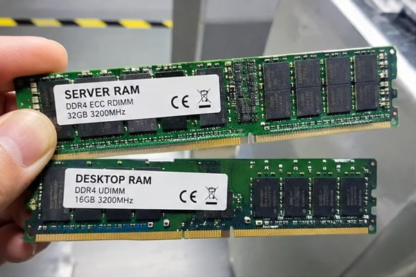
Many hardware buyers assume that matching DDR generations implies universal interoperability across all computing platforms. I regularly consult with enterprise buyers who discover this compatibility barrier only after staging systems fail to initialize on the assembly floor. Let us examine the architectural divisions, electrical mechanics, and system controller realities that separate these hardware categories.
Can server RAM physically fit into a desktop motherboard slot?
System integrators face massive project delays when field technicians force enterprise memory into client desktop motherboards during staging. This basic hardware mismatch leads to unbootable inventory, bent socket pins, and voided component warranties. The physical form factor creates a false sense of security that trips up even experienced purchasing departments.
While unbuffered server memory can mechanically lock into desktop DIMM slots of the same DDR generation, registered server RAM will prevent standard desktop motherboards from completing POST. The pins line up physically, but the internal wiring and memory controllers on desktop boards cannot communicate with enterprise buffering registers.

The illusion of mechanical pin compatibility
I frequently review procurement orders where engineering teams assume mechanical compatibility guarantees system operation. Modern memory standards establish standardized pin layouts across specific generations:
- DDR4 Form Factors: Standard desktop DIMMs and enterprise RDIMMs both feature 288 pins and identical keying notch positions.[^1]
- DDR5 Form Factors: Both consumer and enterprise modules feature 288 pins, though DDR5 shifts power management onto the module via an onboard PMIC.[^2]
The physical key notch prevents users from inserting a DDR4 module into a DDR5 socket. However, this mechanical notch does not differentiate between an enterprise RDIMM and a consumer unbuffered DIMM (UDIMM).
Physical Keying Reality:
[ DDR4 Desktop UDIMM ]  --> 288 Pins --> Fits DDR4 Consumer Slot (POST: Success)
[ DDR4 Server RDIMM  ]  --> 288 Pins --> Fits DDR4 Consumer Slot (POST: Halt / No Boot)
The underlying memory bus architecture explains why this failure occurs. Consumer CPUs integrate basic memory controllers designed to route traces directly from the silicon die to the module DRAM chips. In contrast, enterprise RDIMMs place a dedicated hardware register chip between the memory controller and the DRAM packages.
When a standard desktop processor attempts to poll an RDIMM, it cannot drive the register. The CPU registers an electrical fault or a missing memory module, and the platform halts at power-on self-test (POST).
| Attribute | Desktop UDIMM | Server RDIMM | Server LRDIMM |
|---|---|---|---|
| Physical Pin Count (DDR4/DDR5) | 288 Pins | 288 Pins | 288 Pins |
| Command / Address Register | Absent | Present (Hardware Buffer) | Present (Hardware Buffer) |
| Data Bus Buffer | Absent | Absent | Present (Data Buffers) |
| Consumer Desktop Boot Support | Full Native Support | Complete Failure to Boot | Complete Failure to Boot |
| Target Deployment | Client Workstations | Enterprise Servers | High-Density Compute Nodes |
Why does server RAM use ECC architecture while desktop memory does not?
Silent data corruption threatens financial databases, ERP records, and automated infrastructure pipelines without triggering visible operating system warnings. Single-bit memory errors quietly corrupt active records until storage volumes become irrecoverable. Enterprise infrastructure relies on specialized error mitigation that consumer workstations completely omit.
Server RAM incorporates Error-Correcting Code (ECC) circuitry to detect and correct single-bit memory flips in real time without interrupting active operations. Standard desktop memory lacks the extra physical DRAM chip and parity data paths, meaning consumer platforms crash or silently save corrupted values when electrical interference flips a bit.
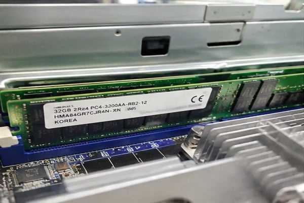
Mitigating bit flips under enterprise duty cycles
Consumer desktops run intermittent duty cycles. Users reboot client workstations daily or weekly, which purges residual memory faults. In our server manufacturing and validation lines, we test server platforms designed to run continuously for five to seven years under heavy thermal and electrical loads.
Under continuous operational profiles, background radiation, electromagnetic interference, and thermal stress produce random bit flips.[^3] These events are called single-event upsets (SEUs).[^4]
An uncorrected bit flip in a consumer PC might crash a spreadsheet or close a local web browser. In contrast, a bit flip in an enterprise virtualization host can corrupt:
- Database balance ledgers across enterprise resource planning systems.
- In-flight storage metadata writes across a SAN or NAS storage array.
- Hypervisor kernel memory, triggering ungraceful host reboots across dozens of guest machines.
Operational Reality: A single unhandled memory fault on a production database node halts business operations. The cost of five minutes of cluster downtime eclipses any margin savings achieved by buying non-ECC consumer memory.
Standard Memory (8-bit bus without parity):
[Byte: 8 Data Bits] ----------------------------> Host Controller (No Verification)

ECC Memory (72-bit bus with Hamming Code check):
[Byte: 8 Data Bits] + [Parity Bit] -------------> Host Controller (Real-Time Correction)
The 64-bit versus 72-bit bus architecture
Standard desktop memory channels operate on a 64-bit data bus per channel. An enterprise ECC module widens this data bus to 72 bits by adding an auxiliary physical memory chip to the printed circuit board.[^5]
The onboard system leverages an algorithm known as Hamming code.[^6] As data writes to the module, the memory controller calculates parity checksums and writes them to the ninth memory chip.
During read operations, the controller recalculates the checksum. If a cosmic ray or transient voltage variance flips a single binary bit from a zero to a one, the ECC engine corrects the bad bit on the fly. If two bits flip simultaneously within the same memory word, the module detects the multi-bit error and triggers a controlled system panic to prevent corrupt data from writing to non-volatile storage.
DDR5 memory adds "on-die ECC" across both consumer and enterprise tiers, but buyers must not confuse this mechanism with true end-to-end ECC.[^7] On-die ECC only corrects bit errors inside the DRAM silicon die itself. True server RAM provides side-band ECC that protects the entire data path as signals travel across the motherboard traces between the memory controller and the DIMM module.
Does server RAM offer faster processing speeds than desktop RAM?
Marketing teams frequently equate enterprise equipment with raw processing speed and lower operating latencies. Buyers often pay high premiums for enterprise hardware under the false impression that it will instantly accelerate application responsiveness. Evaluating memory solely through module megatransfers leads to disappointing performance gains and flawed procurement models.
Server RAM does not provide faster raw processing speed or lower memory latency than consumer desktop memory. In fact, server memory operates with slightly higher absolute latency because the onboard register chips and real-time ECC calculations add small processing delays to ensure absolute signal stability and data integrity.
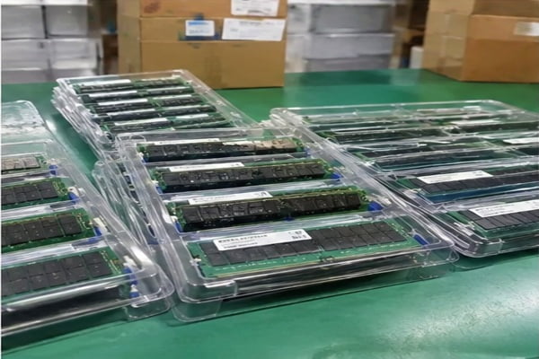
Latency penalties versus sustained channel stability
In high-performance gaming desktops, hardware enthusiasts prioritize aggressive memory timings, low CAS latency (CL), and extreme clock overclocks. In enterprise server design, our priorities are inverted. We prioritize signal integrity, high operating temperatures, deterministic data buses, and multi-year component lifecycles over peak burst speeds.
The physical components responsible for enterprise stability inevitably introduce a latency penalty:
- Register Buffer Delay: An RDIMM incorporates a Register Clock Driver (RCD). The RCD buffers command and address signals before routing them to individual DRAM packages. This buffer isolates the CPU memory controller from electrical capacitance, but it delays address transfers by approximately one clock cycle.[^8]
- Parity Inspection Overhead: Real-time Hamming code generation and error-checking logic require compute cycles within the memory controller, adding minor latency to memory read sequences.
- Conservative Jedec Timings: Consumer RAM frequently leverages Intel XMP or AMD EXPO factory overclocks. Enterprise memory runs strictly within conservative JEDEC specifications[^9] to ensure full platform margins across varying thermal environments.
Throughput scaling under high capacity
Where server RAM genuinely outperforms desktop alternatives is aggregate system bandwidth under maximum memory footprints. When a desktop user installs four high-density unbuffered modules on a consumer motherboard, the memory controller suffers severe electrical loading. Consumer motherboards often downclock memory speeds from DDR5-5600 down to DDR5-4400 or lower to prevent signal degradation across the shared bus.
Enterprise server platforms avoid this degradation. Registered buffers handle the electrical capacitance load, allowing enterprise systems to maintain stable channel speeds even when driving two DIMMs per channel across eight distinct memory channels.
| Metric | High-End Consumer Desktop RAM | Enterprise Server RDIMM |
|---|---|---|
| Typical Clock Speeds | DDR5-6000 to DDR5-7200+ (Overclocked) | DDR5-4800 to DDR5-5600 (JEDEC Spec) |
| Absolute Latency | Low (~10–12 ns) | Moderate (~14–16 ns) |
| Memory Channel Topologies | Dual-Channel (2 Channels) | Octa-Channel (8 Channels) or 12-Channel[^10] |
| Peak Aggregate Bandwidth | ~80–90 GB/s | Up to 400–460 GB/s |
| Overclocking Profiles | Supported (XMP / EXPO) | Unsupported (Strict Stability Focus) |
How does registered buffer design help server RAM scale to higher capacities?
IT departments routinely struggle to scale standard desktop motherboards past modest memory limits without triggering random system crashes. Memory bus lines face physical trace limits that break down as engineers attach more memory chips to the bus. High-capacity computing environments demand advanced memory buffering architectures to scale capacities reliably.
Registered buffer design allows server RAM to scale to massive capacities by electrically isolating the memory chips from the CPU memory controller. The onboard register takes over the electrical load of command and address signals, enabling an enterprise processor to drive dozens of memory modules simultaneously without degrading high-speed bus signals.
Mitigating electrical bus loading with RDIMMs and LRDIMMs
To understand why enterprise platforms scale to multi-terabyte footprints, you must evaluate the electrical capacitance of a motherboard trace. Every memory die soldered onto a memory stick acts as an electrical load on the CPU memory controller.
On a standard desktop, consumer processors support only two memory channels, with a maximum of two DIMMs per channel (2DPC). If you attach four high-density modules:
- The host memory controller must drive dozens of individual DRAM chips directly.
- Signal reflections and electrical noise increase on the data traces.
- The motherboard BIOS drops clock speeds to maintain operational signal margins.
- Total system capacity caps out at 128 GB or 192 GB on typical modern consumer hardware.
Enterprise platforms solve this bus-loading bottleneck through specialized memory topologies:
Registered DIMMs (RDIMMs)
RDIMMs incorporate a Register Clock Driver (RCD) chip placed directly in the center of the module. The CPU memory controller sends command and address instructions directly to this single register.
The register regenerates and drives the electrical signals across the memory module chips. The CPU memory controller sees only a single electrical load per module for command signals, freeing up its signal budget to drive up to 16 or 24 module slots per processor socket.
Load-Reduced DIMMs (LRDIMMs)
In hyper-converged virtualization clusters and AI training nodes, even standard RDIMMs eventually encounter electrical capacitance limits on their high-speed data lines. Load-Reduced memory solves this by replacing the simple RCD register with advanced data buffers.
These buffers intercept both control lines and individual data lines. LRDIMMs convert multi-rank physical architectures into logical ranks[^11], allowing platforms to scale up to 4 TB, 8 TB, or higher across enterprise dual-socket server platforms.
Registered Architecture Layout:
[ CPU Memory Controller ]
          |
   (Single Trace Load)
          v
  [ Central RCD Buffer ]
    /    |
[DRAM][DRAM][DRAM][DRAM] (Locally Buffered Traces)
Frequently Asked Questions
Can you use unbuffered ECC RAM in a normal desktop?
Some desktop motherboards support unbuffered ECC RAM (ECC UDIMM), particularly on AMD Ryzen consumer platforms[^12] and select workstation chipsets. However, the motherboard BIOS must explicitly enable ECC parity reporting. If the platform lacks native BIOS firmware support, the module will either operate in standard non-ECC mode or fail to boot entirely.
Will desktop RAM work in an enterprise rackmount server?
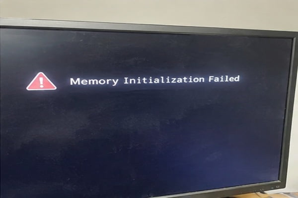
Most enterprise rackmount servers reject standard desktop RAM. Enterprise server chipsets designed for Intel Xeon or AMD EPYC platforms expect registered memory modules (RDIMMs or LRDIMMs). If you install consumer unbuffered non-ECC modules into these systems, the server management controller (BMC) flags an invalid memory configuration and refuses to complete initialization.
What happens if you mix server RAM and desktop RAM together?
You cannot mix registered server memory and unbuffered desktop memory within the same system. Memory controllers cannot toggle between buffered and unbuffered signal pathways simultaneously. Mixing RDIMMs and UDIMMs leads to immediate POST boot halts, memory initialization errors, or fatal platform configuration alarms across all enterprise and consumer platforms.
Why is server RAM typically more expensive than desktop RAM?
Server memory costs more because it incorporates extra physical silicon packages, including dedicated ECC parity chips and specialized Register Clock Drivers (RCD). Furthermore, enterprise memory modules undergo rigorous extended thermal burn-in screening, validated trace matching, and low-volume industrial quality-assurance testing to guarantee multi-year operational reliability under nonstop enterprise workloads.
Conclusion
Determining whether server RAM fits your hardware strategy requires looking past physical slot mechanics and analyzing platform architecture, signal buffering, and workload risk. Consumer desktop memory serves client office computers well by delivering low local latency at accessible costs. In contrast, mission-critical infrastructure mandates registered buffers and comprehensive ECC data protection to maintain uptime and scale across high-density computing clusters.
Investing in unmatched memory hardware causes hardware initialization failures and stalls IT deployments. I advise teams to confirm platform compatibility lists, memory channel configurations, and registered buffer support across all processor and motherboard specifications before releasing capital. Contact our server engineering and procurement specialists today to configure enterprise-grade computing platforms matched specifically to your data center requirements.
[^1]: "DDR4 SDRAM", https://en.wikipedia.org/wiki/DDR4_SDRAM. JEDEC standard JESD79-4 defines the 288-pin physical layout and key notch dimensions for DDR4 memory modules, confirming mechanical pin-count identity across unbuffered and registered variants. Evidence role: definition; source type: institution. Supports: DDR4 unbuffered and registered DIMMs share a 288-pin interface and standardized mechanical keying.. [^2]: "How Power Management Works on DDR5 Memory - Oreton", https://oretonstorage.com/it/blog/ddr5-pmic-explained-how-power-management-works-on-ddr5-memory. According to JEDEC standard JESD79-5 for DDR5 SDRAM, power management circuitry has transitioned from host system motherboards directly onto DIMM modules via dedicated PMICs. Evidence role: mechanism; source type: institution. Supports: DDR5 memory modules incorporate an onboard Power Management Integrated Circuit to regulate supply voltages directly.. [^3]: "DRAM Errors in the Wild: A Large-Scale Field Study", https://www.cs.toronto.edu/~bianca/papers/sigmetrics09.pdf. Schroeder, Pinheiro, and Weber (2009) evaluated DRAM error rates across thousands of servers in Google's data centers, finding that over 8% of DIMMs suffered memory errors annually, demonstrating the necessity of ECC. Evidence role: statistic; source type: paper. Supports: Enterprise servers experience substantial rates of DRAM bit errors under continuous production workloads.. [^4]: "Single-event upset", https://en.wikipedia.org/wiki/Single-event_upset. Ziegler et al. (1996) demonstrated that atmospheric cosmic-ray neutrons and alpha particles induce charge collection that flips semiconductor logic states, formalizing the taxonomy of single-event upsets. Evidence role: definition; source type: paper. Supports: Atmospheric radiation and thermal disturbances cause soft errors termed single-event upsets in silicon DRAM.. [^5]: "ECC memory", https://en.wikipedia.org/wiki/ECC_memory. University computer architecture materials explain that classic ECC DIMMs utilize a 72-bit data path, allocating 64 bits for standard payload data and 8 bits for error-correcting codes. Evidence role: mechanism; source type: education. Supports: Hardware ECC implementations widen the memory bus to 72 bits to accommodate 8 parity and syndrome bits alongside 64 data bits.. [^6]: "Hamming code", https://en.wikipedia.org/wiki/Hamming_code. Richard Hamming's foundational error-correcting codes, extended into single-error-correction double-error-detection (SECDED) matrices, provide the algorithm underlying hardware-level DRAM ECC logic. Evidence role: mechanism; source type: paper. Supports: Hardware memory ECC implementations use extended Hamming codes (SECDED) for single-bit correction and double-bit error detection.. [^7]: "ECC memory", https://en.wikipedia.org/wiki/ECC_memory. JEDEC specifications differentiate DDR5 on-die ECC, which corrects internal silicon bit errors during refresh cycles, from full sideband ECC, which requires additional parity data lines across the bus. Evidence role: mechanism; source type: institution. Supports: On-die ECC in DDR5 functions solely within the physical DRAM die to mitigate internal cell defects rather than securing the channel bus.. [^8]: "Registered memory", https://en.wikipedia.org/wiki/Registered_memory. Memory architecture research confirms that RDIMMs trade a single clock cycle of latency at the Register Clock Driver to regenerate address and command signals before they reach the DRAM chips. Evidence role: mechanism; source type: research. Supports: A Register Clock Driver (RCD) introduces an inherent one-cycle clock delay to re-drive command and address lines.. [^9]: "JEDEC memory standards", https://en.wikipedia.org/wiki/JEDEC_memory_standards. The JEDEC Solid State Technology Association publishes standardized electrical, timing, and thermal profiles that enterprise server vendors enforce to maintain validation and stability across multi-socket configurations. Evidence role: expert_consensus; source type: institution. Supports: Enterprise server platforms restrict memory timing to standardized JEDEC profiles to ensure electrical determinism.. [^10]: "Multi-channel memory architecture", https://en.wikipedia.org/wiki/Multi-channel_memory_architecture. Microprocessor architectural analyses of modern enterprise platforms (such as AMD EPYC 9004 and Intel 4th/5th Gen Xeon) document native memory controllers scaling up to 12 memory channels per CPU. Evidence role: mechanism; source type: research. Supports: Enterprise server processor architectures integrate memory controllers supporting 8 to 12 memory channels per socket.. [^11]: "What is the difference between 'Number of ranks per slot' ...", https://community.altera.com/kb/knowledge-base/what-is-the-difference-between-%C2%91number-of-ranks-per-slot%C2%92-and-%C2%91number-of-chip-se/343788. Engineering analyses of enterprise memory explain that LRDIMMs buffer both control and data lines to synthesize physical ranks into fewer logical ranks, mitigating capacitive loading on the memory controller. Evidence role: mechanism; source type: research. Supports: LRDIMMs utilize data buffers to perform rank multiplication, presenting multiple physical DRAM ranks as fewer logical ranks.. [^12]: "Which AM4 Motherboards Support ECC Memory for the ...", https://www.reddit.com/r/homelab/comments/1f0gxyk/which_am4_motherboards_support_ecc_memory_for_the/. Technical specifications for AMD Ryzen desktop processors verify architectural support for ECC UDIMMs, although active error reporting remains contingent on motherboard firmware implementation. Evidence role: case_reference; source type: other. Supports: AMD Ryzen desktop processors retain integrated hardware support for unbuffered ECC memory modules.. Scope note: Motherboard manufacturers implement Ryzen ECC support inconsistently across consumer product tiers.
发表回复